Method of cutting high-hardness material with multi-wire saw

A high-hardness, wire-saw technology, applied in the direction of metal sawing equipment, stone processing tools, stone processing equipment, etc., can solve problems such as not easy, to achieve the suppression of cutting wire breakage, good sharpness, reduce bending and warping The effect of music

Active Publication Date: 2015-07-22
HITACHI METALS LTD
View PDF9 Cites 5 Cited by
  • Summary
  • Abstract
  • Description
  • Claims
  • Application Information

AI Technical Summary

Problems solved by technology

However, compared with the mass-produced and widely used silicon wafers, it is not easy to cut high-hardness materials with high processing accuracy and finish them into wafers with high flatness.

Method used


Image

  • Method of cutting high-hardness material with multi-wire saw
  • Method of cutting high-hardness material with multi-wire saw
  • Method of cutting high-hardness material with multi-wire saw

Examples


Embodiment

[0074] Hereinafter, an experimental example in which an ingot of a high-hardness material is cut by the cutting method of this embodiment and warpage of a wafer, etc. is studied will be described.

[0075] As an ingot of a high-hardness material, a columnar single-crystal sapphire ingot with a diameter of 150 mm (6 inches) was prepared by cutting out a wafer having the r-plane as a main surface. The ingot was severed using a multi-wire saw, fixed abrasive cutting wire, and cutting fluid as indicated below.

[0076] Multi-wire saw: Multi-wire saw MWS-34 by Takatori

[0077] Cutting wire: diamond electrodeposition cutting wire produced by Allied-material

[0078] (diameter of cutting line: 180μm, average diameter of abrasive grains: 35μm)

[0079] Cutting fluid: DKW-2 produced by Allied-material

[0080] The thickness of the sliced ​​wafer, the maximum contact total length a of the ingot and the dicing wire, the continuous travel distance b, and the new wire discharge amount ...


PUM

PropertyMeasurementUnit
Vickers hardnessaaaaaaaaaa

Abstract

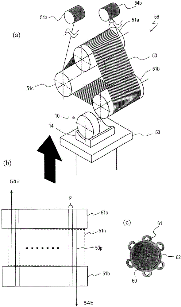
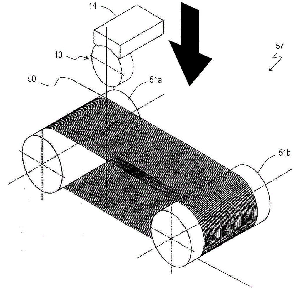
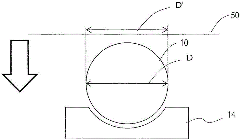
In a method of cutting a high-hardness material with a multi-wire saw, an ingot of the high-hardness material is sliced into a plurality of wafers by cutting the ingot at multiple points simultaneously with the multi-wire saw. The method comprises repeating a run cycle of reciprocating motion of a wire of the multi-wire saw so that the relationships (1) c1≧20, given C1=b / a and (2) 0.35≰c2≰1.55, given c2=d / a are satisfied, where a is a maximum total contact length defined as a sum of the lengths of the ingot as projected onto multiple cut points when projecting the ingot onto the wire in a direction in which the ingot is going to be cut, b is a continuous travel distance of the wire, and d is a length of the wire newly fed in each said run cycle.

Description

technical field [0001] The present invention relates to a method for cutting high hardness materials using a multi-wire saw. Background technique [0002] In recent years, silicon carbide semiconductors have attracted attention as new semiconductor materials. Silicon carbide semiconductors have greater insulation breakdown electric field, electron saturation drift rate and thermal conductivity than silicon semiconductors. Therefore, research and development of power devices capable of operating at a higher temperature and at a higher speed than conventional silicon devices using silicon carbide semiconductors are actively being carried out. Among them, since electric motors used in electric two-wheeled vehicles, electric vehicles, and hybrid vehicles are controlled by AC drives or inverters, attention has been paid to the development of high-efficiency switching elements used in such applications. . In order to realize such a power device, a single crystal silicon carbide...

Claims


Application Information

Patent Timeline
Patent Type & Authority Applications(China)
IPC IPC(8): B28D5/04
CPCB23D61/185B28D1/08B28D5/045
Inventor 近藤祯彦宫地章
Owner HITACHI METALS LTD
Why Eureka
Try Eureka