Switch control circuit with booster

a control circuit and booster technology, applied in logic circuits, logic circuit coupling arrangements, pulse techniques, etc., can solve the problems of reducing circuit reliability and breaking down of sampling switches, and achieve the effect of increasing circuit reliability and internal resistan

Active Publication Date: 2019-03-19
CSMC TECH FAB2 CO LTD
View PDF15 Cites 0 Cited by
  • Summary
  • Abstract
  • Description
  • Claims
  • Application Information

AI Technical Summary

Benefits of technology

[0006]In the above switch control circuit, the voltage boosting circuit can boost the operating voltage outputted by the power source by a preset value, to form a switch control signal and then output the switch control signal to the inverting circuit. The inverting circuit can determine whether or not to output the switch control signal to the switch circuit according to the first clock control signal so as to realize the control of on / off of the switch circuit. Since the voltage boosting value of the switch control signal is the preset value, the voltage boosting amount can be controlled and will not vary with the external factors. Therefore, there is no danger that the switch transistor in the switch circuit is broken down while the internal resistance of the switch circuit is reduced, which results in a higher reliability of the circuit.

Problems solved by technology

However, when the system supply voltage is too high or the sampled analog signal has a large voltage range, it is easily caused that the driving voltage on the sampling switch is too high, so as to result in the risk that the sampling switch is broken down, which reduces reliability of the circuit.

Method used


Image

  • Switch control circuit with booster
  • Switch control circuit with booster
  • Switch control circuit with booster

Examples


Embodiment Construction

[0014]Embodiments of the invention are described more fully hereinafter with reference to the accompanying drawings. The various embodiments of the invention may, however, be embodied in many different forms and should not be construed as limited to the embodiments set forth herein. Rather, these embodiments are provided so that this disclosure will be thorough and complete, and will fully convey the scope of the invention to those skilled in the art.

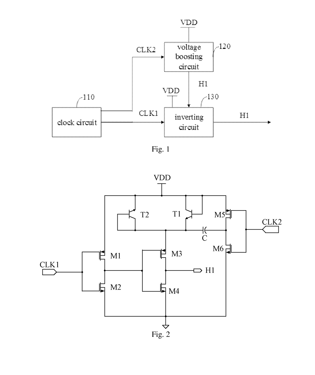
[0015]FIG. 1 is a block diagram of a switch control circuit in an embodiment. The switch control circuit is configured to control on / off of the switch circuit. In the embodiment, the switch control circuit includes a clock circuit 110, a voltage boosting circuit 120 and an inverting circuit 130. The clock circuit 110 is coupled to the voltage boosting circuit 120 and the inverting circuit 130, respectively. The inverting circuit 130 is coupled to the voltage boosting circuit 120 and is also coupled to the switch circuit.

[0016]The clock ...


PUM


Abstract

A switch control circuit includes: a clock circuit (110) configured to generate a first clock control signal (CLK1) and a second clock control signal (CLK2); a voltage boosting circuit (120) configured to receive the second clock control signal (CLK2) and an operating voltage outputted by the power source (VDD); and boost the operating voltage by a preset value to form a switch control signal (H1) under the control of the second clock control signal (CLK2); and an inverting circuit (130) configured to receive the first clock control signal (CLK1) and the switch control signal (H1), and determine whether or not to output the switch control signal (H1) to the switch circuit according to the first clock control signal (CLK1), so as to control on / off of the switch circuit.

Description

CROSS REFERENCE TO RELATED APPLICATIONS[0001]This application is a National Phase filing under 35 U.S.C. § 371 of PCT / CN2016 / 081685 filed May 11, 2016; and this application claims priority to Chinese Application No. 201510452720.6 filed Jul. 28, 2015 under 35 U.S.C. § 119. The entire contents of each application are hereby incorporated by reference.FIELD OF THE INVENTION[0002]The present disclosure relates to the field of circuit control, and particularly relates to a switch control circuit.BACKGROUND OF THE INVENTION[0003]In some high-speed and high-precision signal processing and conversion circuits, it needs some switches to implement the process in which the analog signal is acquired and transmitted. A switch control circuit is configured to control on / off of these switches. Under the premise that the characteristics of the transistors that constitute the switch are constant, the higher the voltage driving the switch is, the smaller the on-resistance of the switch is. The on-res...

Claims


Application Information

Patent Timeline
Patent Type & Authority Patents(United States)
IPC IPC(8): H03K17/06H03K17/10H03K19/0175H03K17/687H03K17/16
CPCH03K17/6871H03K17/102H03K19/017545H03K17/687H03K2217/94H03K17/6872H03K19/00H03K2217/0054
Inventor LUO, CHUAN
Owner CSMC TECH FAB2 CO LTD
Why Eureka
Try Eureka