
Organic light emitting display device and repair method thereof

a technology of light-emitting display device and organic light-emitting display device, which is applied in the direction of organic semiconductor devices, semiconductor devices, instruments, etc., can solve the problems of degrading the production yield increasing the probability of occurrence of defective pixels in the display panel of organic light-emitting display devices including the aforementioned pixels p, and enhancing the display quality of 3d images. , to achieve the effect of enhancing th

Active Publication Date: 2019-04-30
LG DISPLAY CO LTD
View PDF13 Cites 0 Cited by
  • Summary
  • Abstract
  • Description
  • Claims
  • Application Information

AI Technical Summary

Benefits of technology

This patent describes an organic light emitting display device that can improve the quality of 3D images. The device uses a repair structure to compensate for any defective pixels and enhance production yield. Additionally, the device includes a repair structure for preventing bright spots in a 3D image.

Problems solved by technology

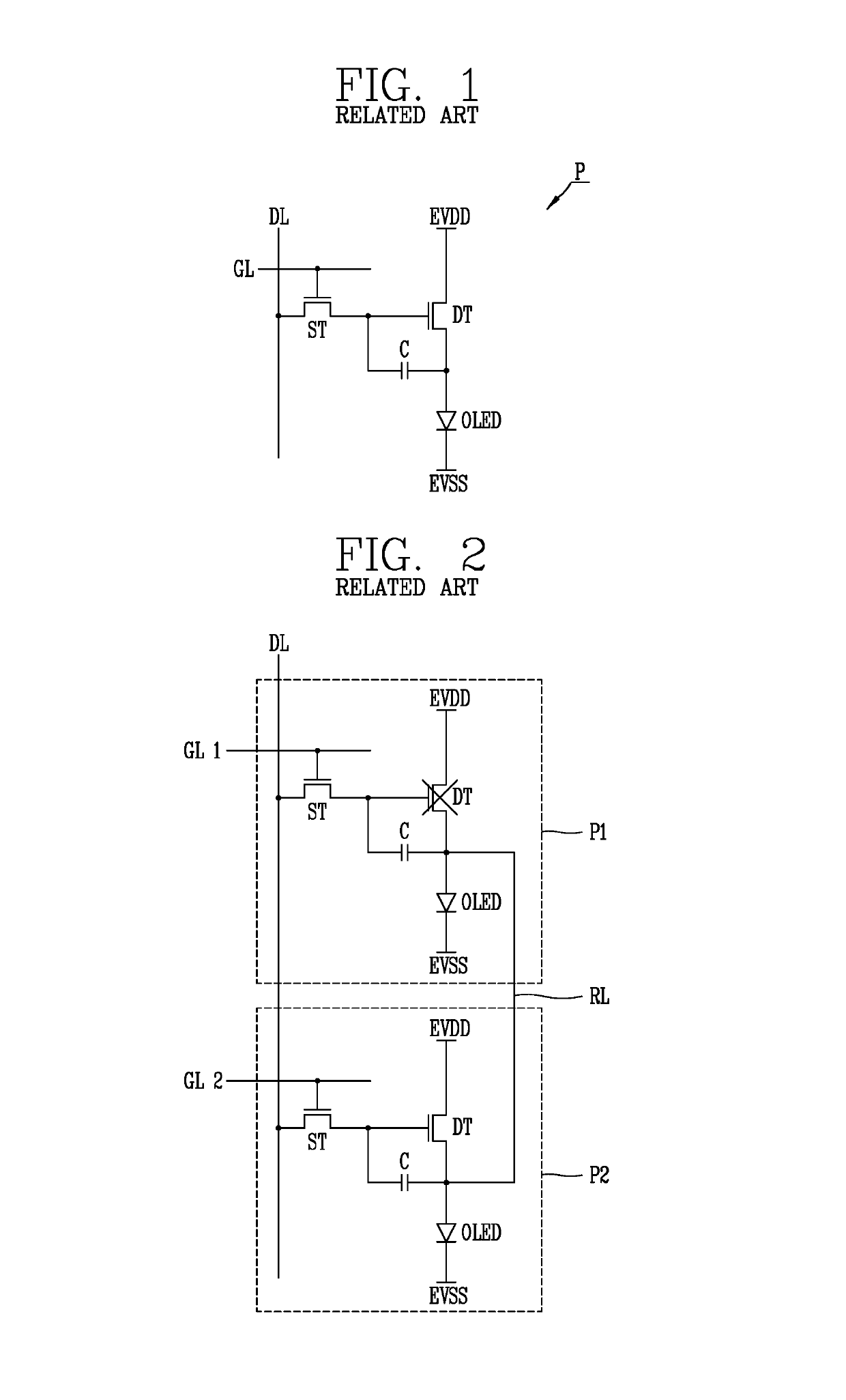
As organic light emitting display devices are increased in size, a probability of occurrence of defective pixels in the display panel of the organic light emitting display device including the aforementioned pixels P is increased.
Also, display panels are discarded due to defective pixels, a production yield of organic light emitting display devices is degraded.
However, in the organic light emitting display device based on the related art pixel repair structure, the display quality is degraded when a 3D image is displayed.

Method used


Image

  • Organic light emitting display device and repair method thereof
  • Organic light emitting display device and repair method thereof
  • Organic light emitting display device and repair method thereof

Examples


Embodiment Construction

[0037]These and other objects of the present application will become more readily apparent from the detailed description given hereinafter. However, it should be understood that the detailed description and specific examples, while indicating preferred embodiments of the invention, are given by way of illustration only, since various changes and modifications within the spirit and scope of the invention will become apparent to those skilled in the art from this detailed description. Like reference numerals designate like elements throughout the specification.

[0038]Hereinafter, an organic light emitting display device and a repair method thereof according to an embodiment of the present disclosure will be described in detail with reference to the accompanying drawings.

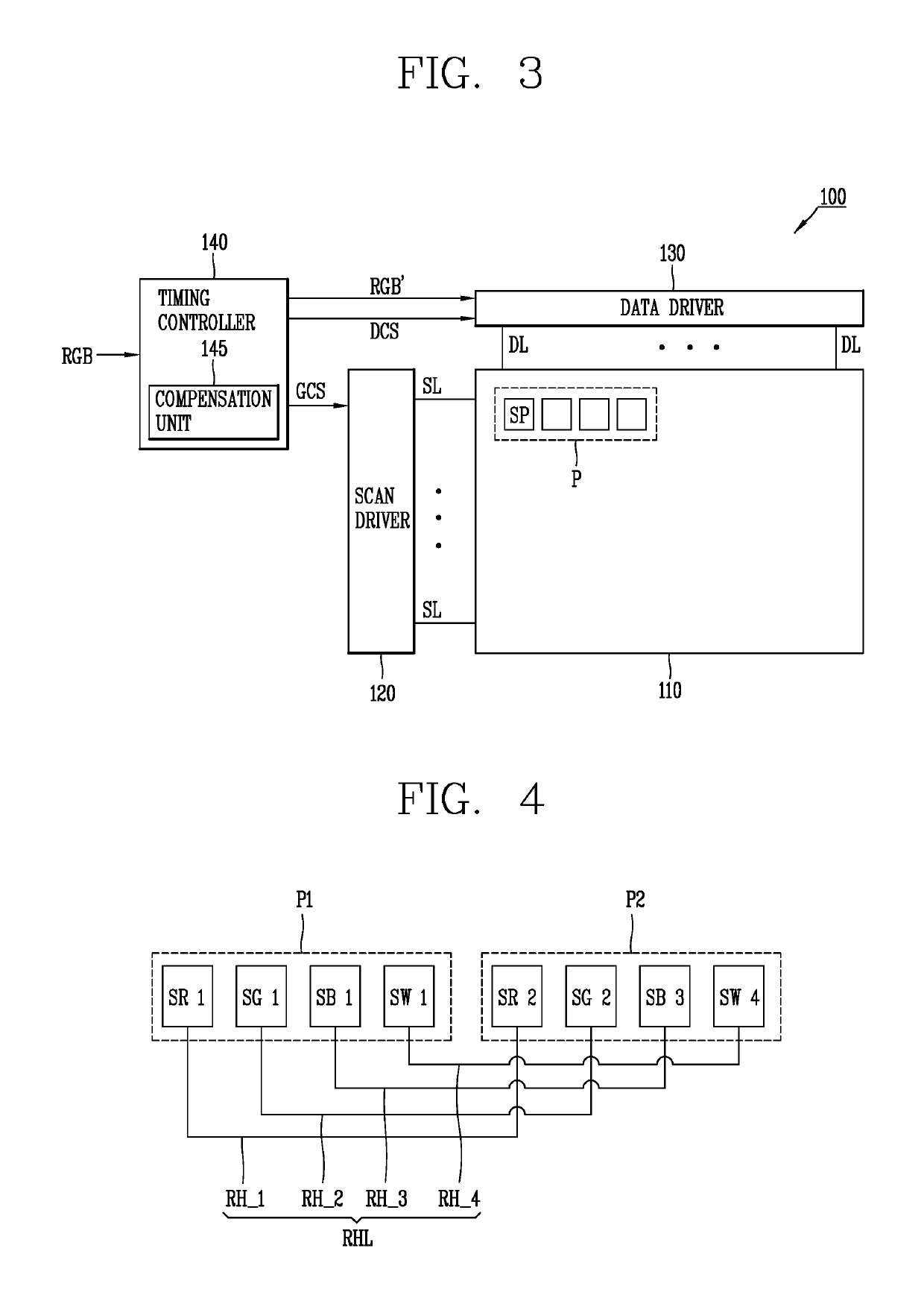
[0039]FIG. 3 is a view illustrating a configuration of an organic light emitting display device according to an embodiment of the present disclosure, and FIG. 4 is a view schematically illustrating a pixel repair struct...


PUM


Abstract

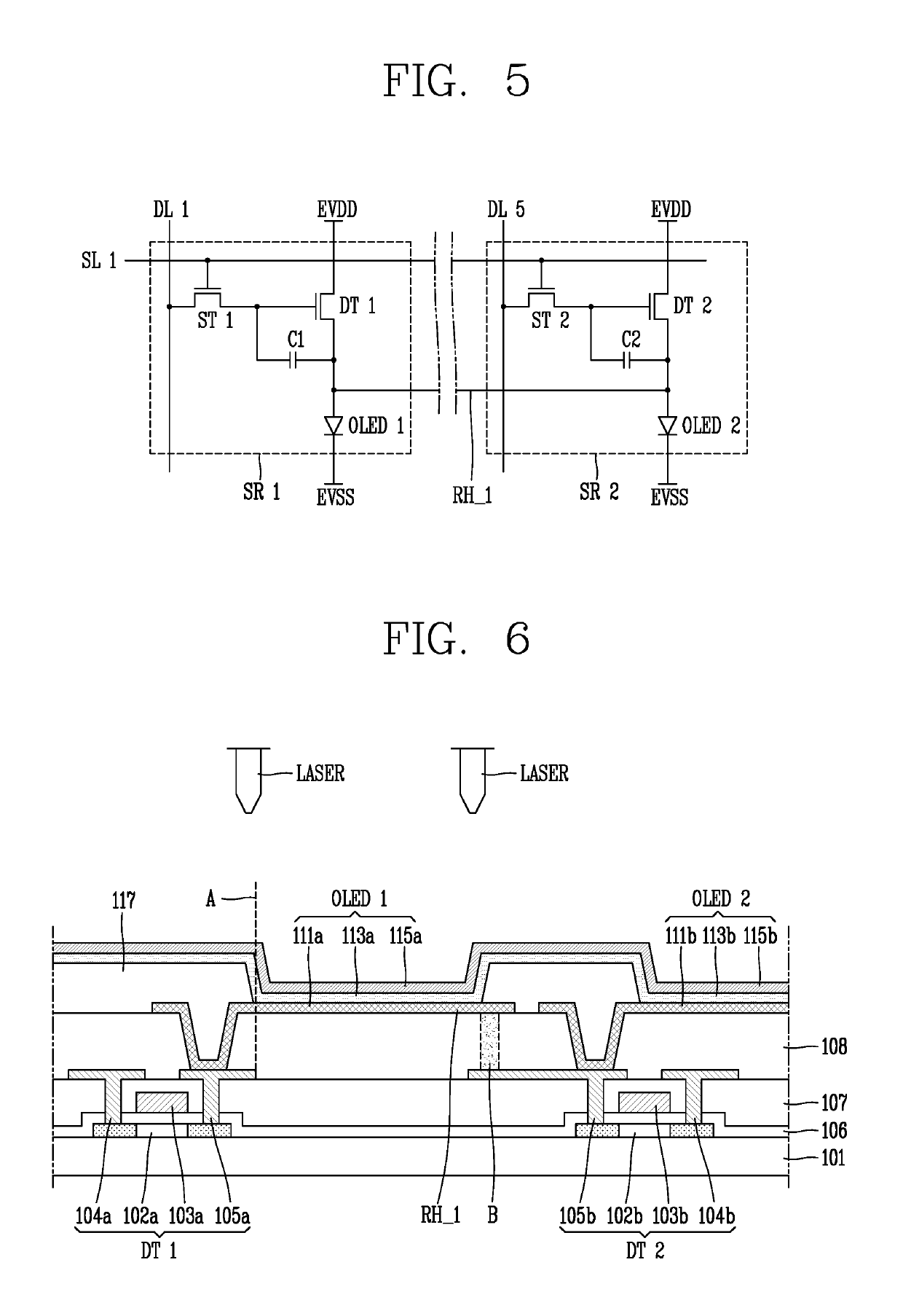
An organic light emitting display device and a method of repairing the device are discussed. According to an embodiment, the device includes a display panel having pixels, each including an OLED in every pixel area defined as scan and data lines intersect with each other and having a repair structure in at least one of horizontal and vertical directions between adjacent pixels by one or more repair lines; a timing controller configured to generate compensation data when a dark spot is generated in one of the plurality of pixels of the display panel, and adjust a magnitude of image data according to the compensation data; and a data driver configured to adjust a magnitude of a data voltage according to the image data adjusted in magnitude, and output the data voltage adjusted in magnitude to the data lines.

Description

CROSS-REFERENCE TO RELATED APPLICATION[0001]Pursuant to 35 U.S.C. § 119(a), this application claims the benefit of earlier filing date and right of priority to Korean Patent Application No. 10-2014-0192565, filed on Dec. 29, 2014, the contents of which is incorporated by reference herein in its entirety.BACKGROUND OF THE INVENTION[0002]Field of the Invention[0003]The present disclosure relates to an organic light emitting display device, and particularly, to an organic light emitting display device having a pixel repair structure and a pixel repair method thereof.[0004]Discussion of the Related Art[0005]Flat panel displays such as a liquid crystal display (LCD), a field emission display (FED), a plasma display panel (PDP), and an organic light emitting display device may replace existing cathode ray tube (CRT) display devices.[0006]Among them, the organic light emitting display device is a self-luminous device which uses an organic light emitting diode (OLED), having advantages in t...

Claims


Application Information

Patent Timeline
Patent Type & Authority Patents(United States)
IPC IPC(8): G09G3/20H01L51/56H01L27/32G09G3/00G09G3/3291G09G3/3233G09G3/3283
CPCG09G3/2003G09G3/003G09G3/3233G09G3/3291H01L27/3248H01L27/3276H01L51/56H01L2251/568G09G3/3283G09G2300/043G09G2300/0426G09G2320/0242G09G2330/08G09G2330/10G09G3/2092G09G3/3208H10K59/351H10K59/123H10K59/131H10K71/861H10K59/84H10K71/00
Inventor LEE, YOONJUKIM, JEONGHWANCHOI, SOOHONGSHIN, HONGJAEPARK, KWANGMOSONG, JAYEON
Owner LG DISPLAY CO LTD
Learn More