
Techniques for indirect optical coupling between an optical input/output port of a subassembly housing and an arrayed waveguide grating (AWG) device disposed within the same

a technology of arrayed waveguide grating and optical input/output port, which is applied in the direction of electromagnetic transceivers, optical waveguide light guides, instruments, etc., can solve the problem of scaling down while maintaining nominal transceiver performan

Active Publication Date: 2019-05-21
APPLIED OPTOELECTRONICS
View PDF14 Cites 4 Cited by
  • Summary
  • Abstract
  • Description
  • Claims
  • Application Information

AI Technical Summary

Problems solved by technology

The desire to provide higher speeds in smaller optical transceiver modules for a lower cost has presented challenges, for example, with respect to maintaining optical efficiency (power), thermal management, insertion loss, and manufacturing yield.
As channel density becomes an increasingly important aspect of optical transceivers, the ability scale-down while maintaining nominal transceiver performance raises numerous non-trivial challenges.

Method used


Image

  • Techniques for indirect optical coupling between an optical input/output port of a subassembly housing and an arrayed waveguide grating (AWG) device disposed within the same
  • Techniques for indirect optical coupling between an optical input/output port of a subassembly housing and an arrayed waveguide grating (AWG) device disposed within the same
  • Techniques for indirect optical coupling between an optical input/output port of a subassembly housing and an arrayed waveguide grating (AWG) device disposed within the same

Examples


Embodiment Construction

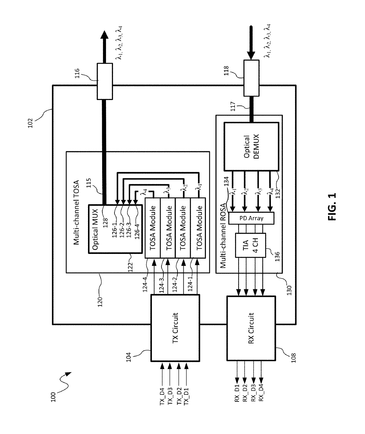
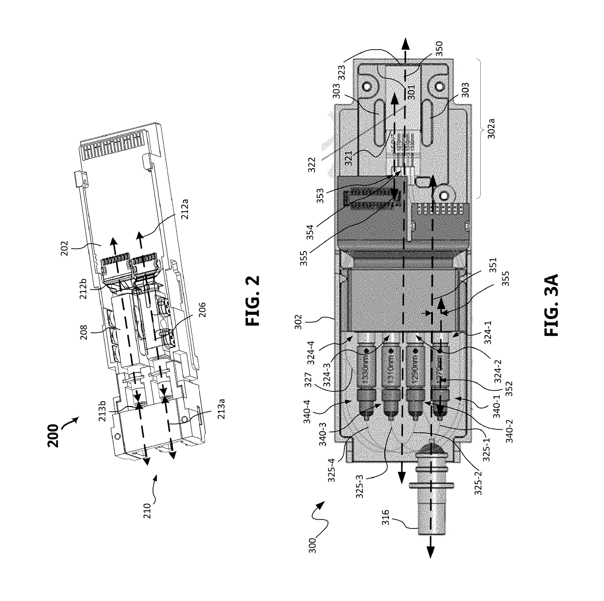
[0012]Optical transceiver devices generally include a housing with various optical components, e.g., receiver optical subassembly (ROSA) modules and transmitter optical subassembly (TOSA) modules, disposed therein for launching and receiving channel wavelengths, and an optical input / output port for optically coupling the optical components to an external transmit and / or receive fiber. The particular position of the input / output ports may be governed by a particular standard. For instance, as shown in FIG. 2, the optical transceiver 200 implements a small-form factor plugging SFFP architecture which includes a pair of optical ports 210, e.g., LC ports, disposed at an end of the housing 202. The particular position of the optical ports 210 limits the position of a multi-channel TOSA 206 and a multi-channel ROSA 208, which are disposed in different sections of the housing 202. For instance, given the space constraints of the housing 202, each of the multi-channel TOSA 206 and ROSA 208 ...


PUM


Abstract

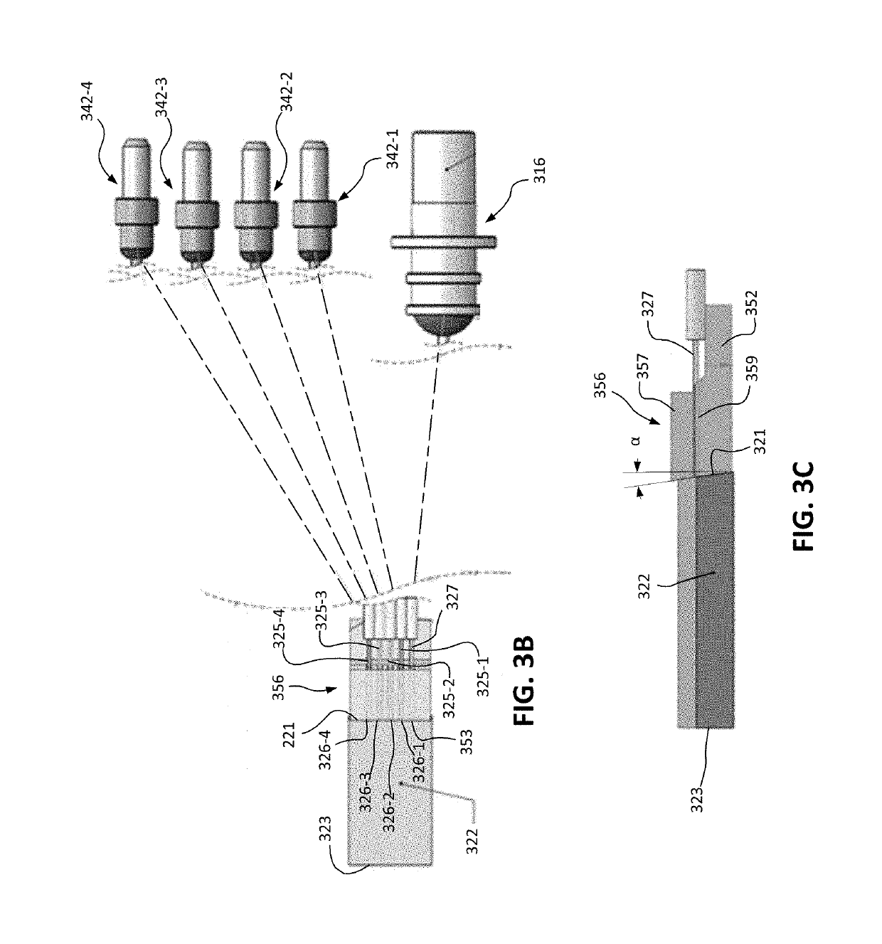
Techniques for flexible coupling between an optical coupling receptacle / port of an optical transceiver housing and optical components within the same are disposed. In an embodiment, an optical transceiver housing includes an intermediate fiber with a first end optically coupled to an optical coupling port and a second end optically coupled to a multiplexer / de-multiplexer device, e.g., an arrayed waveguide grating (AWG) device, PLC splitter, and so on. The intermediate fiber may be routed in the transceiver housing in a manner that and the radius of the bends may be optimized to reduce fiber bending losses. The techniques herein are equally applicable to both ROSA and TOSA modules and may be utilized to achieve flexible coupling for multi-channel transceiver devices.

Description

TECHNICAL FIELD[0001]The present disclosure relates to optical transmitters and transceivers, and more particularly, to techniques for utilizing a single fiber to optically couple an output / input optical port of a subassembly housing to optical components within the same in order to allow for flexible position of the output / input optical port relative to the optical components.BACKGROUND INFORMATION[0002]Optical transceivers are used to transmit and receive optical signals for various applications including, without limitation, internet data centers, cable TV broadband, and fiber to the home (FYI H) applications. Optical transceivers provide higher speeds and bandwidth over longer distances, for example, as compared to transmission over copper cables. The desire to provide higher speeds in smaller optical transceiver modules for a lower cost has presented challenges, for example, with respect to maintaining optical efficiency (power), thermal management, insertion loss, and manufact...

Claims


Application Information

Patent Timeline
Patent Type & Authority Patents(United States)
IPC IPC(8): G02B6/12G02B6/38G02B6/125G02B6/42H04B10/40
CPCG02B6/4246G02B6/125G02B6/4256H04B10/40G02B6/3897G02B2006/12164G02B6/4215G02B6/421G02B6/12019
Inventor HO, I-LUNGPENG, LUOHANLIN, KAI-SHENGMARENTES, ELSIE
Owner APPLIED OPTOELECTRONICS
Learn More