Display device

a display device and display technology, applied in the field of display devices, can solve the problems of increasing operation temperature, reducing product reliability and strength, and over manual procedures, and achieve the effects of reducing components, reducing manufacturing costs, and reducing manufacturing costs

Active Publication Date: 2019-06-11
INNOLUX CORP
View PDF2 Cites 0 Cited by
  • Summary
  • Abstract
  • Description
  • Claims
  • Application Information

AI Technical Summary

Benefits of technology

[0006]An objective of the disclosure is to provide a display device with reduced components. The display device of the disclosure has good assembling accuracy, reworkability and reliability and can be utilized in the automatic assembling process.

Problems solved by technology

First, the above manual procedure needs a lot of time and has larger assembling tolerances.
Besides, the tightness between the metal back plate and the flexible lighting bar can sufficiently affect the heat dissipation efficiency of the LED, so that the LED may have poor heat dissipation so as to cause the increase of operation temperature if bubbles exist in the attaching part.
Second, the flexible lighting bar can be easily bended during the assembling and the LED may be easily contacted by hands, thereby decreasing the product reliability and strength.
Third, the flexible lighting bar must be removed from the metal back plate during the rework procedure, which can also easily cause the deformation of the flexible lighting bar and the loosening of the LED.
Fourth, the automatic machine cannot easily pick up or suck the flexible lighting bar, so that it is hard to carry out the automatic assembling process.

Method used


Image

  • Display device
  • Display device
  • Display device

Examples


Embodiment Construction

[0015]The embodiments of the disclosure will be apparent from the following detailed description, which proceeds with reference to the accompanying drawings, wherein the same references relate to the same elements. Moreover, the drawings of all implementation are schematic, and they do not mean the actual size and proportion. The terms of direction recited in the disclosure, for example up, down, left, right, front, or rear, only define the directions according to the accompanying drawings for the convenience of explanation but not for limitation. The names of elements and the wording recited in the disclosure all have ordinary meanings in the art unless otherwise stated. Therefore, a person skilled in the art can unambiguously understand their meanings.

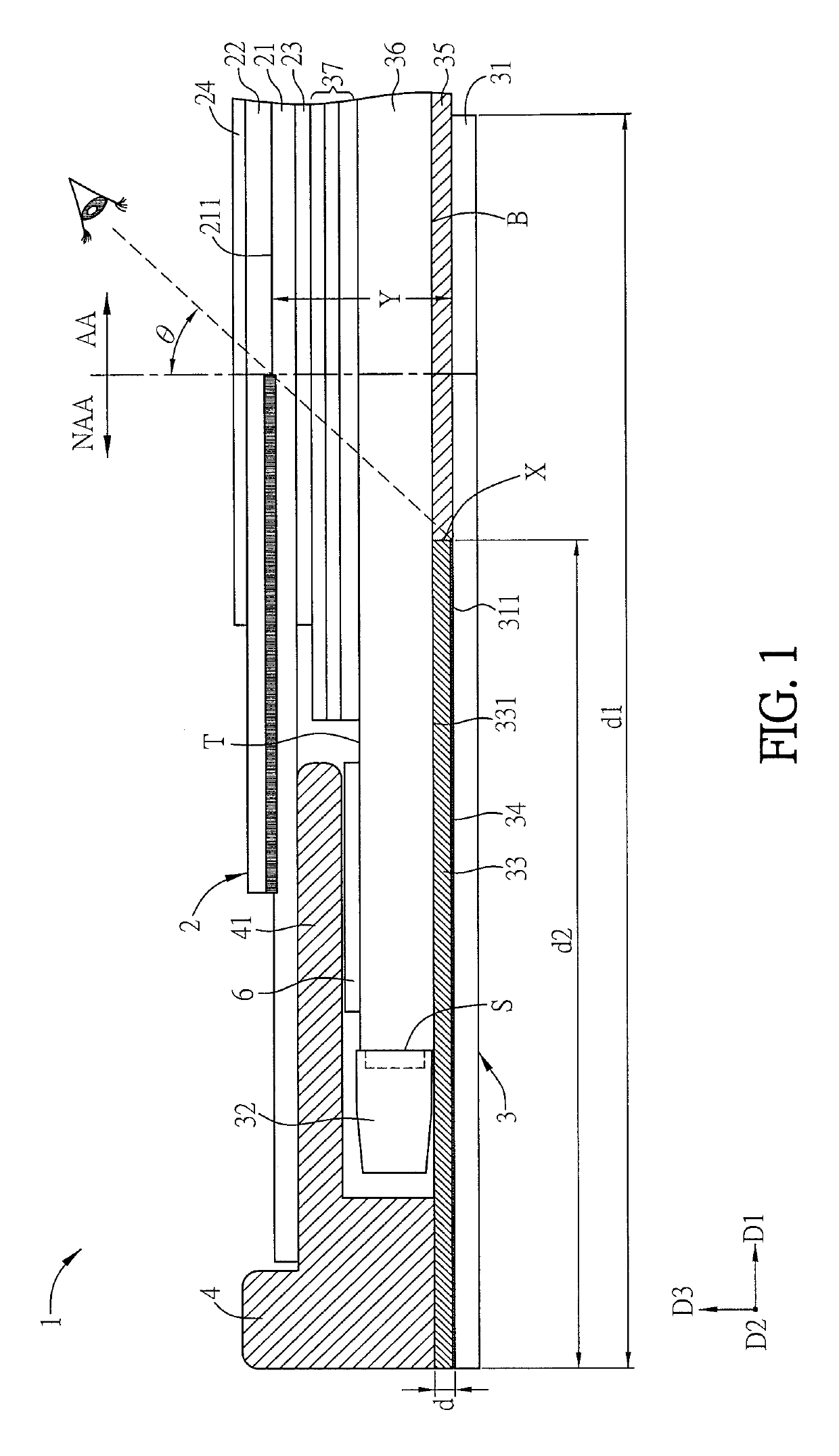
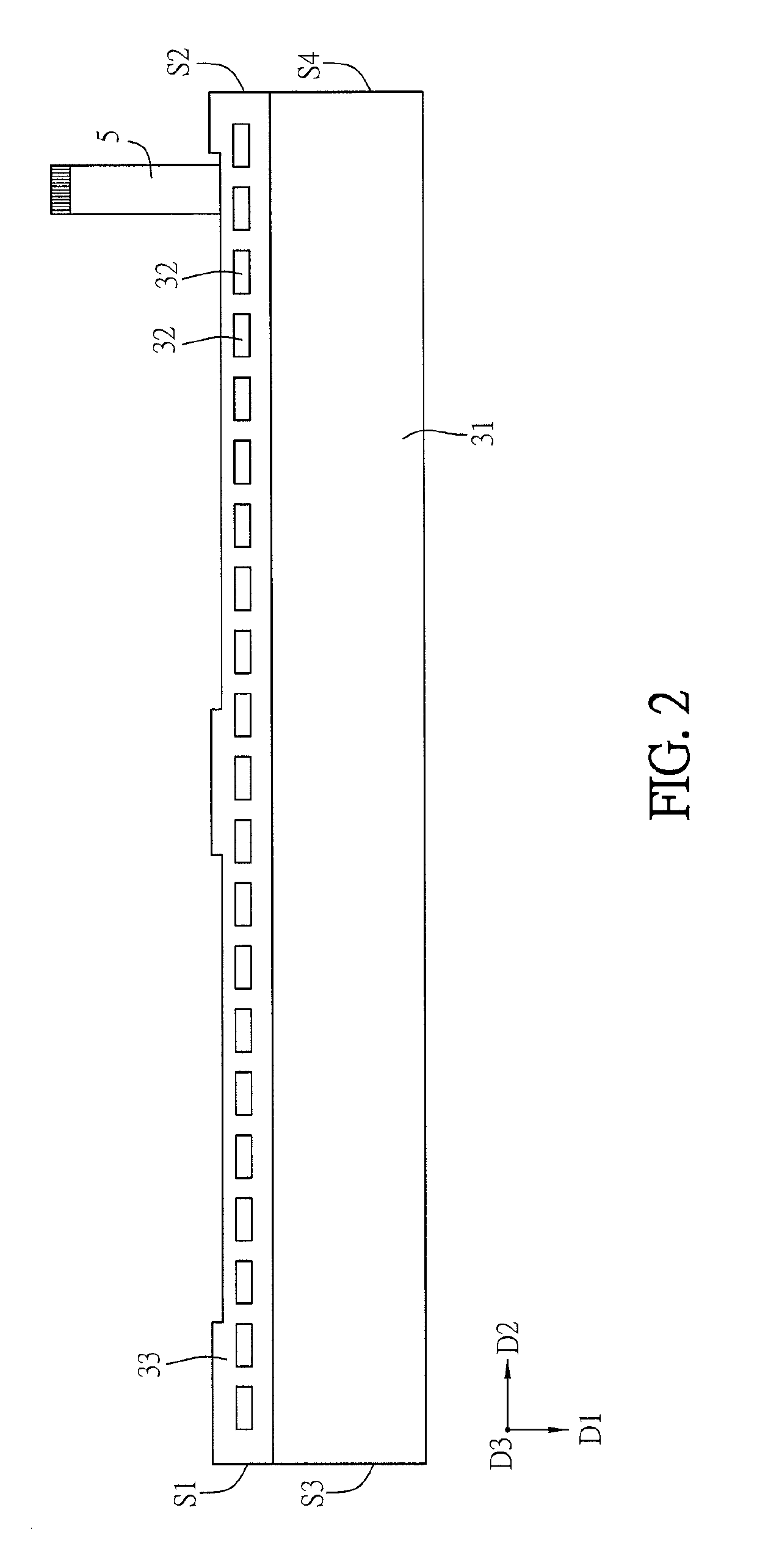
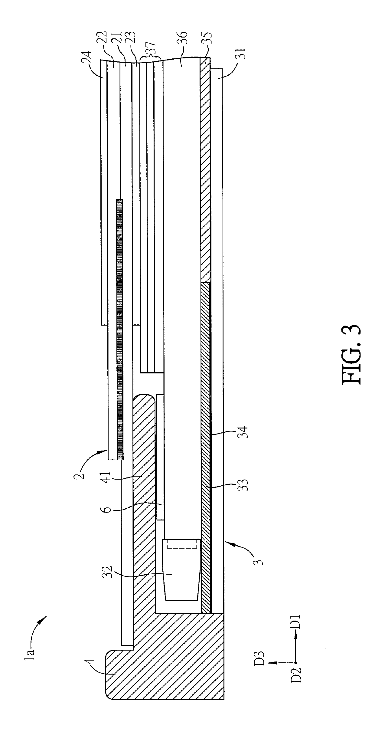
[0016]FIG. 1 is a schematic diagram showing a display device 1 according an embodiment of the disclosure, and FIG. 2 is a top view of a metal substrate 31, a light emitting element 32, and a circuit layer 33 of a backlight module 3 o...


PUM

PropertyMeasurementUnit
widthaaaaaaaaaa
distanceaaaaaaaaaa
thicknessaaaaaaaaaa

Abstract

A display device includes a display panel and a backlight module. The display panel is disposed opposite to the backlight module. The backlight module includes a metal substrate, a light emitting element, a circuit layer, an adhesive layer, a reflective element and a light guiding element. The light emitting element is disposed at one side of the circuit layer facing the light guiding element. The adhesive layer is disposed between the circuit layer and a surface of the metal substrate. The reflective element is disposed adjacent to the circuit layer and the adhesive layer and is located on the surface of the metal substrate. The reflective element is disposed between the metal substrate and the light guiding element. A bottom surface of the adhesive layer and at least a part of a bottom surface of the reflective element are located at a same plane.

Description

CROSS REFERENCE TO RELATED APPLICATIONS[0001]This Non-provisional application claims priority under 35 U.S.C. § 119(a) on Patent Application No(s). 201610714867.2 filed in People's Republic of China on Aug. 24, 2016, the entire contents of which are hereby incorporated by reference.BACKGROUNDTechnical Field[0002]The present disclosure relates to a display device and, in particular, to a flat display device.Related Art[0003]In the recent years, the processes and materials for manufacturing light emitting diodes (LED) have been improved, so that the lighting efficiency of LED is sufficiently enhanced. Different from the general fluorescent lamp or compact lamp, the LED lamp has the features of low power consumption, long lifetime, high safety, short response time, and small size. Accordingly, the LED lamps have been applied to the lighting apparatuses such as the indoor lamps, flashlights, headlights of vehicles, other lighting devices, or the backlight module of flat display device.[...

Claims


Application Information

Patent Timeline
Patent Type & Authority Patents(United States)
IPC IPC(8): F21V8/00G02F1/1368G02F1/1333G02F1/1335
CPCG02B6/0055G02B6/0056G02B6/0083G02B6/0088G02F1/133308G02F2001/133531G02F1/1368G02F1/133514G02F1/133528H01L27/1214G02B6/0085G02F1/133531
Inventor HSIA, KUANG-TECHIU, CHUANG-HSUNCHENG, YU-CHENG
Owner INNOLUX CORP
Why Eureka
Try Eureka