Printed circuit board test coupon for electrical testing during thermal exposure and method of using the same

a printed circuit board and thermal exposure technology, applied in the direction of printed element electric connection formation, inspection/indentification of circuits, instruments, etc., can solve the problems of difficult to get a statistically significant amount of plated holes/vias tested, limited detection of daisy chains,

Active Publication Date: 2019-06-25
RELIABILITY ASSESSMENT SOLUTIONS INC
View PDF4 Cites 5 Cited by
  • Summary
  • Abstract
  • Description
  • Claims
  • Application Information

AI Technical Summary

Problems solved by technology

Daisy chains are limited to detecting these fractures or cracks in an advanced stage, as the volume of copper in the plated hole is significantly greater that the volume of copper in the traces connecting them together in the daisy chain.
Daisy chain test nets cannot electrically differentiate the degree of fractures or cracks in different / multiple plated holes / vias of the test net.
The disadvantage to this method is that it is difficult to get a statistically significant amount of plated holes / vias tested as each test net only provides information on one plated hole / via, whereas daisy chain test nets allow for resistance data to be collected from multiple plated holes / vias in one test net.

Method used


Image

  • Printed circuit board test coupon for electrical testing during thermal exposure and method of using the same
  • Printed circuit board test coupon for electrical testing during thermal exposure and method of using the same
  • Printed circuit board test coupon for electrical testing during thermal exposure and method of using the same

Examples


Embodiment Construction

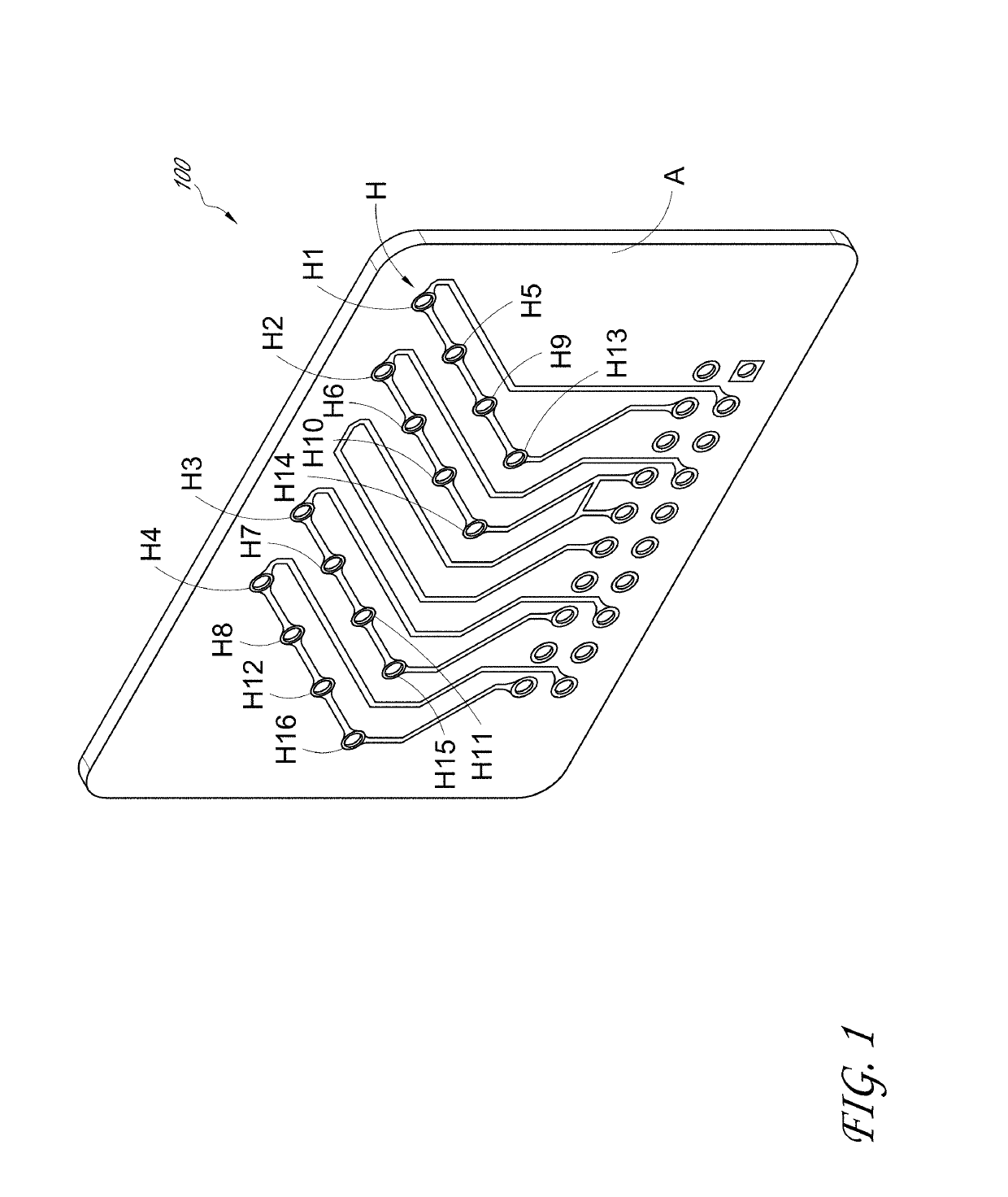
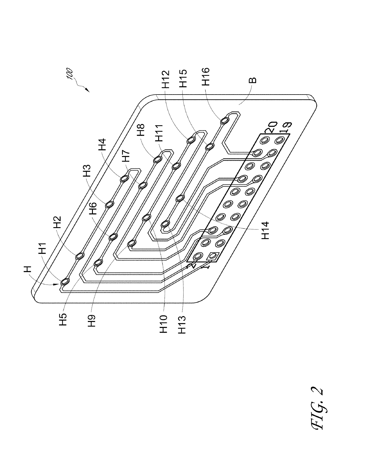
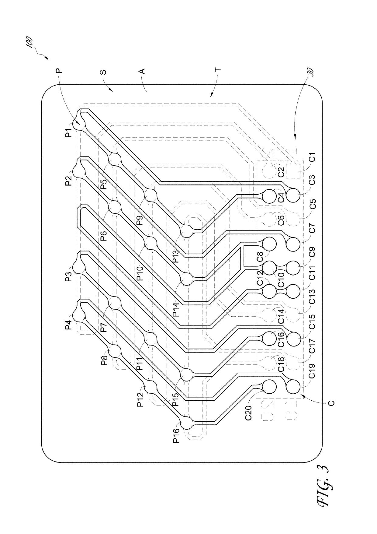
[0019]FIGS. 1-2 show a printed circuit board (PCB) test coupon 100 or the internal layers of a multilayer PCB test coupon for use in electrical testing during thermal exposure. Thermal exposure includes cycling the test coupon 100 between extreme temperatures (e.g., extreme low temperature and extreme high temperature), for example by flowing a fluid (e.g., air) at different temperatures past the test coupon 100 and sensing the resistance of various components of the test coupon 100 through the connector pattern 30.

[0020]The test coupon 100 can be made using the same process used to manufacture the final printed circuit boards which they represent and can have substrate S with plated holes / vias (blind, buried, stacked, through) H, multiple conductive layers, and trace patterns T (e.g., made of copper or other conductive material) that connect to either side of the plated holes / vias H using pads P.

[0021]With continued reference to FIGS. 1-2, the test coupon 100 has an array of sixtee...


PUM


Abstract

A printed circuit board (PCB) test coupon for thermal exposure and electrical testing includes a double sided or multi-layer substrate with a plurality of vias formed within the substrate of the test coupon (blind, buried, stacked vias) or extending through the entire substrate (through hole / via) from a first surface on the first side of the plated hole / via to a second surface on the second side of the plated hole / via. Each of a first plurality of trace patterns interconnect a subset of the plurality of plated holes / vias on the first side of the plated holes / vias, and each of a second plurality of trace patterns interconnect a different subset of the plurality of plated holes / vias on the second side of the plated holes / vias. The first and second pluralities of trace patterns have different patterns and connect to connection points in a connector pattern defined in the substrate. One of the second plurality of trace patterns is configured to measure temperature and two of the second plurality of trace patterns are configured to measure calibration / drift by resistance measurements. The test coupon provides test nets that include a single plated hole / via, and optionally includes daisy chain test nets. A resistance measurement of each plated hole / via (or daisy chain) is provided by connecting 2 wires of a 4-wire kelvin bridge measurement system to the first and second sides of the plated hole / via (or daisy chain) using connection points for one of the first plurality of trace patterns and one of the second plurality of trace patterns that connect to each side of the said plated hole / via (or daisy chain).

Description

INCORPORATION BY REFERENCE TO ANY PRIORITY APPLICATIONS[0001]Any and all applications for which a foreign or domestic priority claim is identified in the Application Data Sheet as filed with the present application are hereby incorporated by reference under 37 CFR 1.57.BACKGROUNDField[0002]The invention is directed to a printed circuit board (PCB) test coupon for use in electrical testing during thermal exposure, and more particularly to a PCB test coupon having a matrix of holes that can be electrically measured with a limited number of test channelsDescription of the Related Art[0003]Electrical testing of plated holes / vias (e.g., through, blind, buried, stacked) in double sided or multilayer printed circuit boards (PCB) to discover electrical reliability involves placing specifically designed test coupons into a thermal cycling environment that sequentially exposes them to hot and cold temperature extremes in cycles causing expansion and contraction of the plated hole / via with eac...

Claims


Application Information

Patent Timeline
Patent Type & Authority Patents(United States)
IPC IPC(8): G01R31/28H05K1/02H05K3/42
CPCH05K1/0268G01R31/2818G01R31/2805H05K3/429G01R31/2817H05K2201/09609H05K2203/162
Inventor NEVES, ROBERT
Owner RELIABILITY ASSESSMENT SOLUTIONS INC
Why Eureka
Try Eureka