
Eureka
For R&D, Eureka makes reading and utilizing patents & technical documents easy.
Eureka AIR
Designed for self-driven R&D workflows. Generate viable solutions, solve complex R&D challenges, empower your innovation with AI.

Eureka Materials
Designed for material experts only. Revolutionize your material R&D, from search, analyze, to developing new materials.

TechResearch
Generate reliable direction feasibility study reports for your R&D in just a few steps.

TechSeek
Discover and master advanced knowledge NOW. Basics, ideas, possibilities, all at once.

TechMind
As an expert in R&D Theories, TechMind can generates customized viable solutions instantly.

TechRisk
Analyze your overall solution with one click, know your potential R&D risks in advance.

TechMonitor
Get weekly tech updates, stay abreast of the latest tech innovations and key insights.
Power-on reset signal generating apparatus and voltage detection circuit thereof
- Summary
- Abstract
- Description
- Claims
- Application Information
AI Technical Summary
Benefits of technology
Problems solved by technology
Method used
Image

Examples
Embodiment Construction
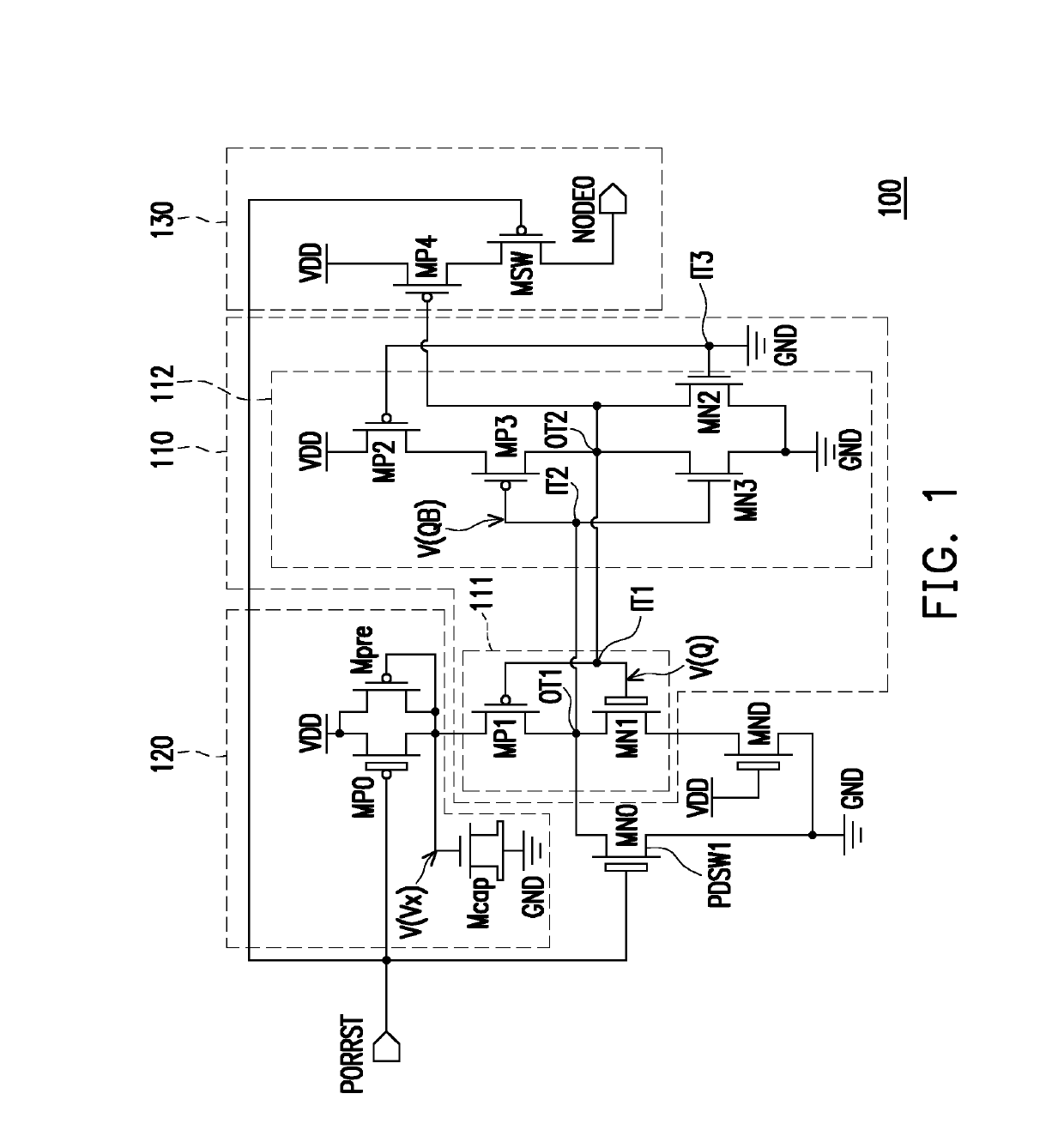
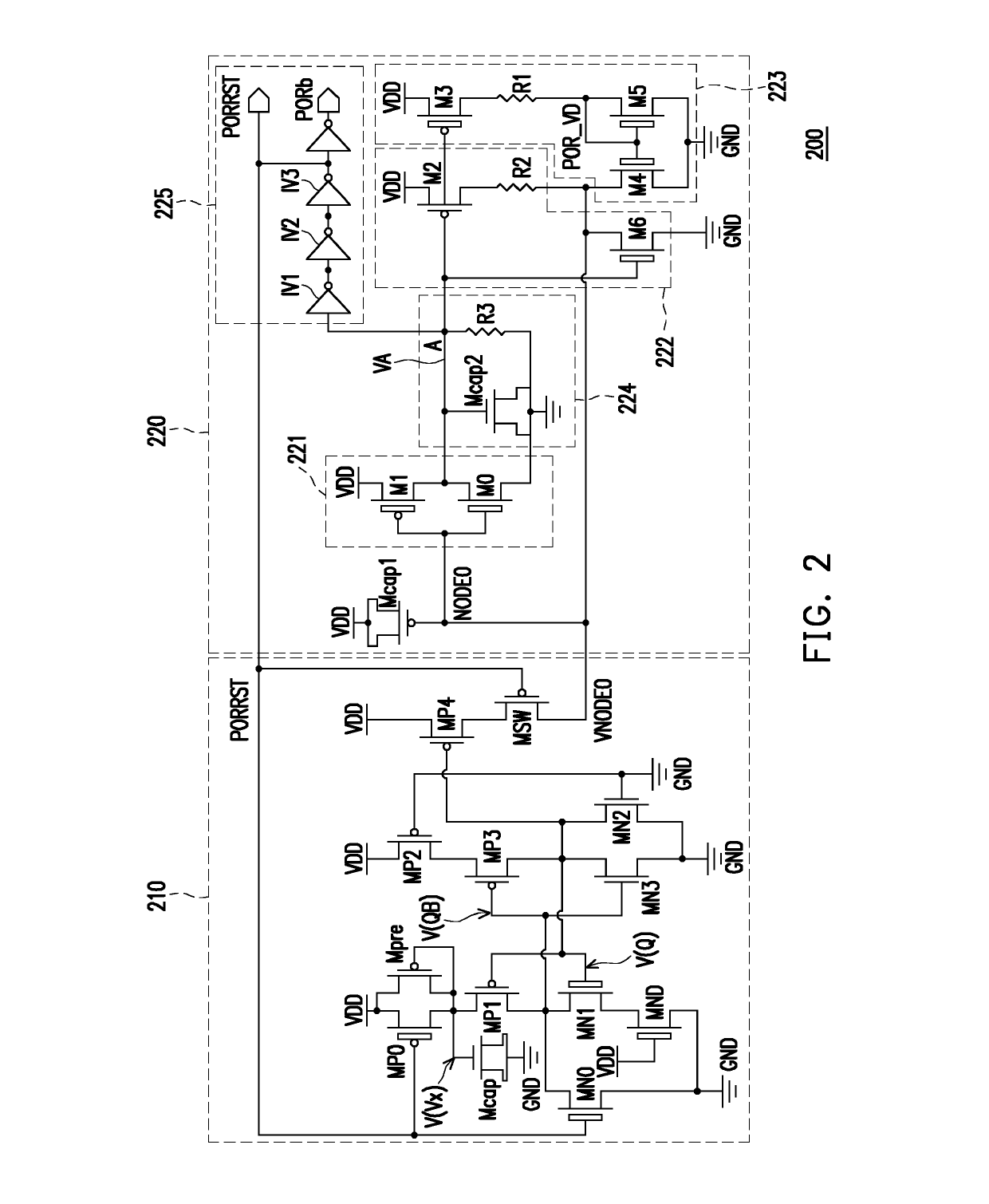
[0013]Please refer to FIG. 1, FIG. 1 is a schematic diagram of a voltage detection circuit according to an embodiment of the present invention. The voltage detection circuit 100 includes a latch circuit 110, a pre-charge circuit 120, an output stage circuit 130, and a pull-down switch PDSW1. The latch circuit 110 has an inverter 111 and an NOR gate circuit 112, and forming an unbalanced latch circuit through the inverter 111 and the NOR gate circuit 112. The input end IT1 of the inverter 111 is coupled to the output end OT2 of the NOR gate circuit 112, the output end OT1 of the inverter 111 is coupled to the input end IT2 of the NOR gate circuit 112, the input end IT3 of the NOR gate circuit 112 receives the reference ground voltage GND.
[0014]In this embodiment, the pre-charge circuit 120 is coupled between the paths of the inverter 111 receiving the power supply voltage VDD. The pre-charge circuit 120 receives the power-on reset signal PORRST and performs a pre-charging action acco...
PUM
 Abstract
Description
Claims
Application Information
 - R&D Engineer
- R&D Manager
- IP Professional
- Industry Leading Data Capabilities
- Powerful AI technology
- Patent DNA Extraction
Browse by: Latest US Patents, China's latest patents, Technical Efficacy Thesaurus, Application Domain, Technology Topic, Popular Technical Reports.
© 2024 PatSnap. All rights reserved.Legal|Privacy policy|Modern Slavery Act Transparency Statement|Sitemap|About US| Contact US: help@patsnap.com