Low profile magnetoresistive imaging sensor array

a low-profile magnetoresistive and imaging sensor technology, applied in the field ofcurency detection, magnetic read head, imaging, can solve the problems of limited fidelity of magnetically printed images, insufficient scanning quality, low scanning speed, etc., and achieve the effect of reducing the distance between the medium and the imaging sensor array and reducing the spacing

Active Publication Date: 2019-08-06
MULTIDIMENSION TECH CO LTD
View PDF25 Cites 0 Cited by
  • Summary
  • Abstract
  • Description
  • Claims
  • Application Information

AI Technical Summary

Benefits of technology

[0008]As for the problem in the prior art of a large spacing between a magnetoresistive imaging sensor array and a medium, the technical solution provided by the present invention to reduce the spacing between the magnetoresistive imaging sensor array and the medium includes: optimizing the arrangement of an application integrated circuit and a magnetoresistive imaging sensing element array, mounting an integrated circuit on a top surface and a bottom surface of a sensing element array substrate and on a top surface and a bottom surface of an ASIC substrate separately, and using the through-the-chip interconnections and other technologies that can reduce the spacing between the magnetoresistive imaging sensor array and the medium to replace bonding pads in the prior art, thereby achieving longitudinal electric connections. Due to the presence of the bonding pad on the sensing element array chip or the sensing element array substrate, the distance between the magnetoresistive imaging sensor array substrate and the bottom surface of a protective casing is increased by 100 to 200 μm, bumps for protection and insulation purposes on the bonding pad further increase this distance, and the typical thickness of a protective casing is 100 to 200 μm. It can be seen that, the new design of the present invention can reduce the distance between the medium and the imaging sensor array by 50%.
[0030]Compared with the prior art, the present invention has the following beneficial effects: the low profile magnetoresistive imaging sensor array of the present invention features good performance, excellent quality and low cost, and has higher spatial resolution, higher signal-to-noise ratio, more compact detecting system, smaller volume and lower cost and is firmer and more durable as compared with the existing products of the same type.

Problems solved by technology

However, with rapid development of reduction printing and scanning technologies, there is a need and an opportunity to read printed matters smaller than 25 μm, and moreover, the existing digital scanning speed is not high and the scanning quality is not good enough.
Therefore, a magnetic scanning head with higher spatial resolution is really needed, a magnetic scanning system capable of providing a magnetically printed image of high fidelity is also needed, and the fidelity of the magnetically printed image is limited to relative geometric positions of elements on the sensing system, the quantity of induction elements on the scanning head and the requirement of distributing the magnetic field of the image along multiple coordinate axes.
When the spacing aspect ratio is less than 1:1, the imaging is easy; and when the aspect ratio is greater than 1:1, image signals from two adjacent objects become blurred, and it is difficult to distinguish the image.

Method used


Image

  • Low profile magnetoresistive imaging sensor array
  • Low profile magnetoresistive imaging sensor array
  • Low profile magnetoresistive imaging sensor array

Examples


Embodiment Construction

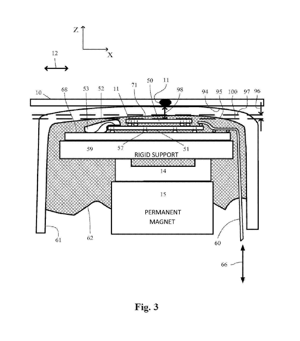
[0043]The present invention is described in detail below with reference to embodiments and the accompanying drawings.

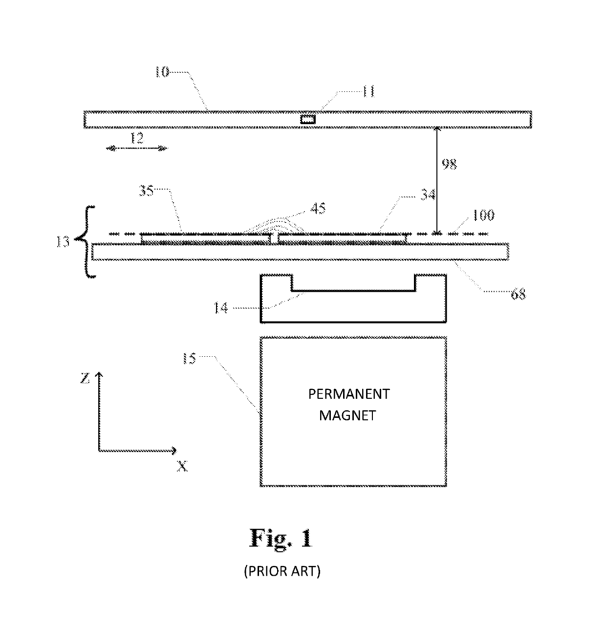
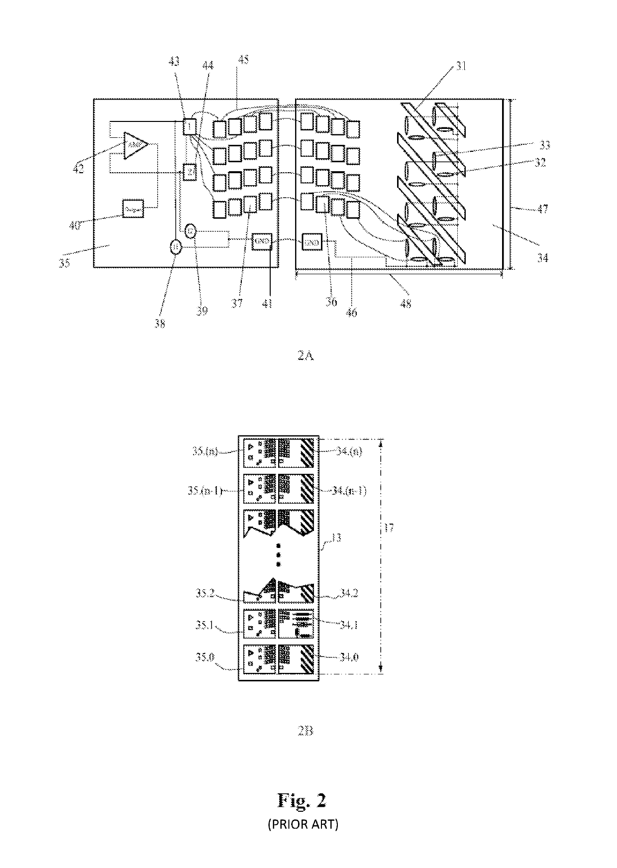
[0044]FIG. 1 and FIG. 2 show a magnetoresistive imaging sensor array in the prior art and the defect thereof as well as basic knowledges for designing and using the magnetoresistive imaging sensor array. The description about the design of the low profile magnetoresistive imaging sensor array in the present invention starts from FIG. 3. Specifically, the magnetoresistive imaging sensor array is a magnetic medium scanning head. FIG. 1 shows a medium 10 passing through the sensor array 13, where the medium 10 may be an entire bill or an entire piece of paper moving along an axial medium moving direction 12, and this axis is parallel to an X-axis 1. A standard coordinate system is shown in the lower right corner of FIG. 1, and the coordinate system has the X-axis 1, a Y-axis 2 (along a paper inward direction) and a Z-axis 3. A common motor and / or roller is used to drive ...


PUM


Abstract

A low profile magnetoresistive imaging sensor array based on the principle of magnetic induction, which reduces a distance between a medium imaging sensor array and a medium by optimizing the arrangement of an application integrated circuit and a sensing element array and using an electric connection technology which can reduce the distance between the medium imaging sensor array and the medium, thereby increasing the resolution of the existing medium imaging sensor. The low profile magnetoresistive imaging sensor array includes a sensing element array and an application integrated circuit, and also includes a circuit which provides a power for the sensing element array, a magnetoresistive sensing element array selection circuit, a signal amplification circuit, a digitizer, a memory circuit, and a microprocessor. Additionally, the sensing element array includes at least one magnetoresistive sensing element.

Description

PRIORITY CLAIM TO RELATED APPLICATIONS[0001]This application is a U.S. national stage application filed under 35 U.S.C. § 371 from International Application Serial No. PCT / CN2014 / 095246, which was filed 29 Dec. 2014, and published as WO2015 / 101244 on 9 Jul. 2015, and which claims priority to Chinese Application No. 201310750924.9, filed 31 Dec. 2013, which applications and publication are incorporated by reference as if reproduced herein and made a part hereof in their entirety, and the benefit of priority of each of which is claimed herein.TECHNICAL FIELD[0002]The present invention relates to the technical fields of currency detection, magnetic read heads, imaging and the like, and in particular, to a low profile magnetoresistive imaging sensor array and chip-level packaging.BACKGROUND ART[0003]The maximum diameter of a physical area for high-resolution dotting on paper is 25 μm. An electronic image detector reads such a minute image from a medium and converts the image into an ele...

Claims


Application Information

Patent Timeline
Patent Type & Authority Patents(United States)
IPC IPC(8): G01R31/02G01R33/07G01R33/09G06K9/18G06K9/20G06V30/224
CPCG01R33/091G01R33/072G06K9/209G06K9/186G01R33/09G06V30/2253
Inventor TONDRA, MARK C.XUE, SONGSHENGDEAK, JAMES GEZAJIN, INSIKSHEN, WEIFENG
Owner MULTIDIMENSION TECH CO LTD
Why Eureka
Try Eureka