Multi-bit computing circuit for computing-in-memory applications and computing method thereof

a multi-bit computing and application technology, applied in the direction of information storage, static storage, digital storage, etc., can solve the problems of large overhead, write disturb, and inability to realize both negative and positive weights in the same bl

Active Publication Date: 2019-08-13
NATIONAL TSING HUA UNIVERSITY
View PDF5 Cites 14 Cited by
  • Summary
  • Abstract
  • Description
  • Claims
  • Application Information

AI Technical Summary

Benefits of technology

The present patent provides a multi-bit computing circuit and method for computing-in-memory applications. The circuit includes a memory cell array and a capacitor sharing unit. The memory cells store weights, which are connected to a bit line, a word line, and an input port. The circuit can compute a cell output signal by combining the input value and the weights. The capacitive sharing unit includes switches, capacitors, and a sense amplifier. The switches connect the cell output signals to the capacitors, which are located between the switches and the sense amplifier. The sense amplifier generates a total operational value, which is equal to the input value multiplied by the weights. The circuit can apply multiple voltage levels to the input value, which drives the memory cells and the capacitive sharing unit to produce the total operational value. The technical effects of the invention include efficient use of memory space and improved performance of computing-in-memory applications.

Problems solved by technology

An extra digital-to-analog convertor (DAC) is required to support multi-bit MAC operation, which results in larger area overhead.
Therefore, it is impossible to realize both negative and positive weights in the same BL.
Moreover, in a conventional 6T SRAM, there exists a write disturb issue when a large number of WLs are activated.

Method used


Image

  • Multi-bit computing circuit for computing-in-memory applications and computing method thereof
  • Multi-bit computing circuit for computing-in-memory applications and computing method thereof
  • Multi-bit computing circuit for computing-in-memory applications and computing method thereof

Examples


Embodiment Construction

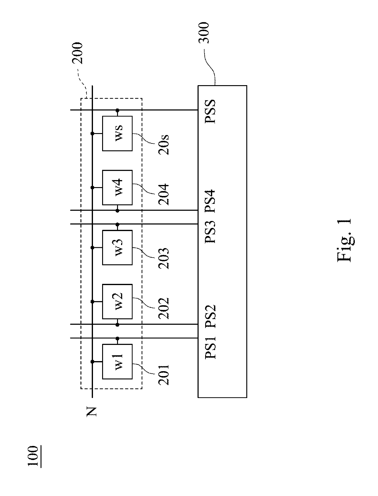
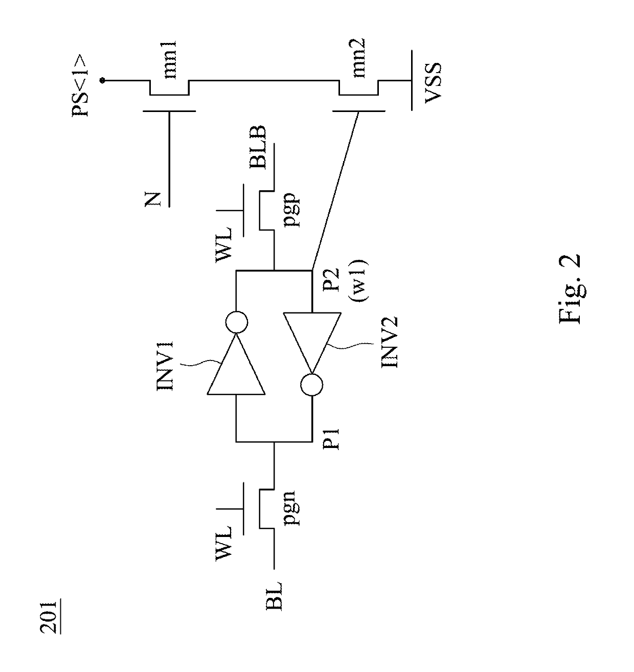
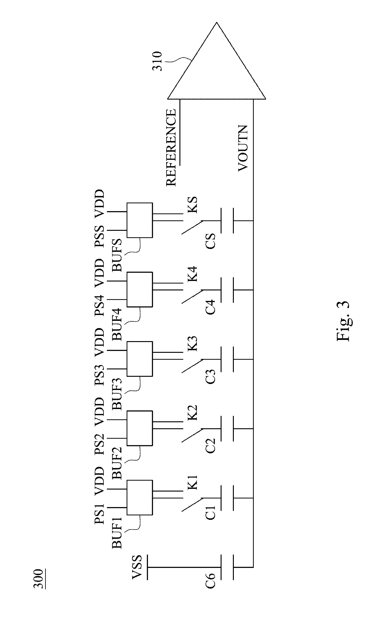
[0015]FIG. 1 shows a block diagram of a multi-bit computing circuit 100 for computing-in-memory applications according to one embodiment of the present disclosure; FIG. 2 shows a circuit diagram of a memory cell 201 of the multi-bit computing circuit 100 for the computing-in-memory applications of FIG. 1; FIG. 3 shows a circuit diagram of a capacitor sharing unit 300 of the multi-bit computing circuit 100 for the computing-in-memory applications of FIG. 1; and FIG. 4 shows timing diagrams of voltages of the switches K1, K2, K3, K4, KS of the capacitor sharing unit 300 of FIG. 3. The multi-bit computing circuit 100 for the computing-in-memory applications is controlled by a first bit line BL, a second bit line BLB, a word line WL and an input port N. The input port N transmits an input value which is a multi-bit input value. The multi-bit input value is given sequentially via the input port N. The multi-bit computing circuit 100 for the computing-in-memory applications includes a mem...


PUM


Abstract

A multi-bit computing circuit for computing-in-memory applications is controlled by an input port and includes a memory cell array and a capacitor sharing unit. The memory cell array includes a plurality of memory cells connected to the input port. The memory cells store a weight which is formed in two's complement. The capacitor sharing unit includes a plurality of switches, a plurality of capacitors and a sense amplifier. The switches are electrically connected to the memory cells, respectively. The capacitors are electrically connected to the switches, respectively. The sense amplifier is electrically connected to the capacitors and generates a total operational value. The capacitors are located among the switches and the sense amplifier, and the switches are switched to enable the total operational value to be equal to the input value multiplied by the weight. The present disclosure utilizes 8T SRAM cells without an extra DAC structure.

Description

BACKGROUNDTechnical Field[0001]The present disclosure relates to a multi-bit computing circuit for computing-in-memory applications and a computing method thereof. More particularly, the present disclosure relates to a multi-bit computing circuit for computing-in-memory applications and a computing method thereof which are capable of solving the problem of the write disturb without an extra digital-to-analog convertor.Description of Related Art[0002]In these years, due to the industrial growth of mobile device, medical electrical equipment, portable storage, etc., requirement of memory with low power, high speed and high density is increased. In one conventional computing-in-memory structure, it often has to turn on a large number of word lines to realize the multiply and accumulate (MAC) operation with multi-bit inputs and weights. An extra digital-to-analog convertor (DAC) is required to support multi-bit MAC operation, which results in larger area overhead. In a static random acc...

Claims


Application Information

Patent Timeline
IPC IPC(8): G11C11/00G11C11/418G11C11/419G11C11/56G11C11/412
CPCG11C11/419G11C11/412G11C11/56G11C11/418G11C7/1006G11C7/062G11C11/24G11C7/16G11C11/54
Inventor SI, XINCHANG, MENG-FAN
Owner NATIONAL TSING HUA UNIVERSITY
Why Eureka
Try Eureka