Trench-based diode and method for manufacturing such a diode

a technology of diodes and clamps, which is applied in the field of clamps and diodes for manufacturing such a diode, can solve the problems of reducing the efficiency of the system, affecting the performance of the system, and the limitation of the maximum cutoff voltage of the diodes, so as to reduce the unsatisfactory correlation, reduce the loss, and reduce the effect of resistan

Active Publication Date: 2019-10-01
ROBERT BOSCH GMBH
View PDF4 Cites 0 Cited by
  • Summary
  • Abstract
  • Description
  • Claims
  • Application Information

AI Technical Summary

Benefits of technology

[0008]The present invention makes it possible to reduce the unsatisfactory correlation between the cutoff current and the forward voltage. The diode according to the present invention may have very small resistance in the flow direction, associated with low losses and a resulting very high efficiency. In addition, it has a low cutoff current. The diodes according to the present invention may also be used for voltage limitation. The power semiconductor diode according to the present invention may also be packaged in a press-fit diode housing and used for efficient rectification in motor vehicle AC generators.

Problems solved by technology

In systems which are designed for relatively low system voltages, which is the case, for example, in motor vehicle generator diodes, the maximum cutoff voltage of the diodes may be additionally limited.
The forward voltage of PN diodes results in conducting-state power losses and thus in an efficiency degradation of the system, for example, a generator.
The conducting-state power losses result in undesirable heating of the components, which must be counteracted by complex measures for dissipating heat from the rectifier to the surroundings using heat sinks and / or fans.
The existing approaches are either relatively complex, as in the case of actively controlled power transistors, and / or they are difficult to integrate into a single housing, for example, into a press-fit diode housing for motor vehicle generators, or they have only a limited effect.
Thus, in the case of pure diode approaches, it has hitherto not been possible to overcome the correlation between forward voltage and the cutoff currents.

Method used


Image

  • Trench-based diode and method for manufacturing such a diode
  • Trench-based diode and method for manufacturing such a diode
  • Trench-based diode and method for manufacturing such a diode

Examples


Embodiment Construction

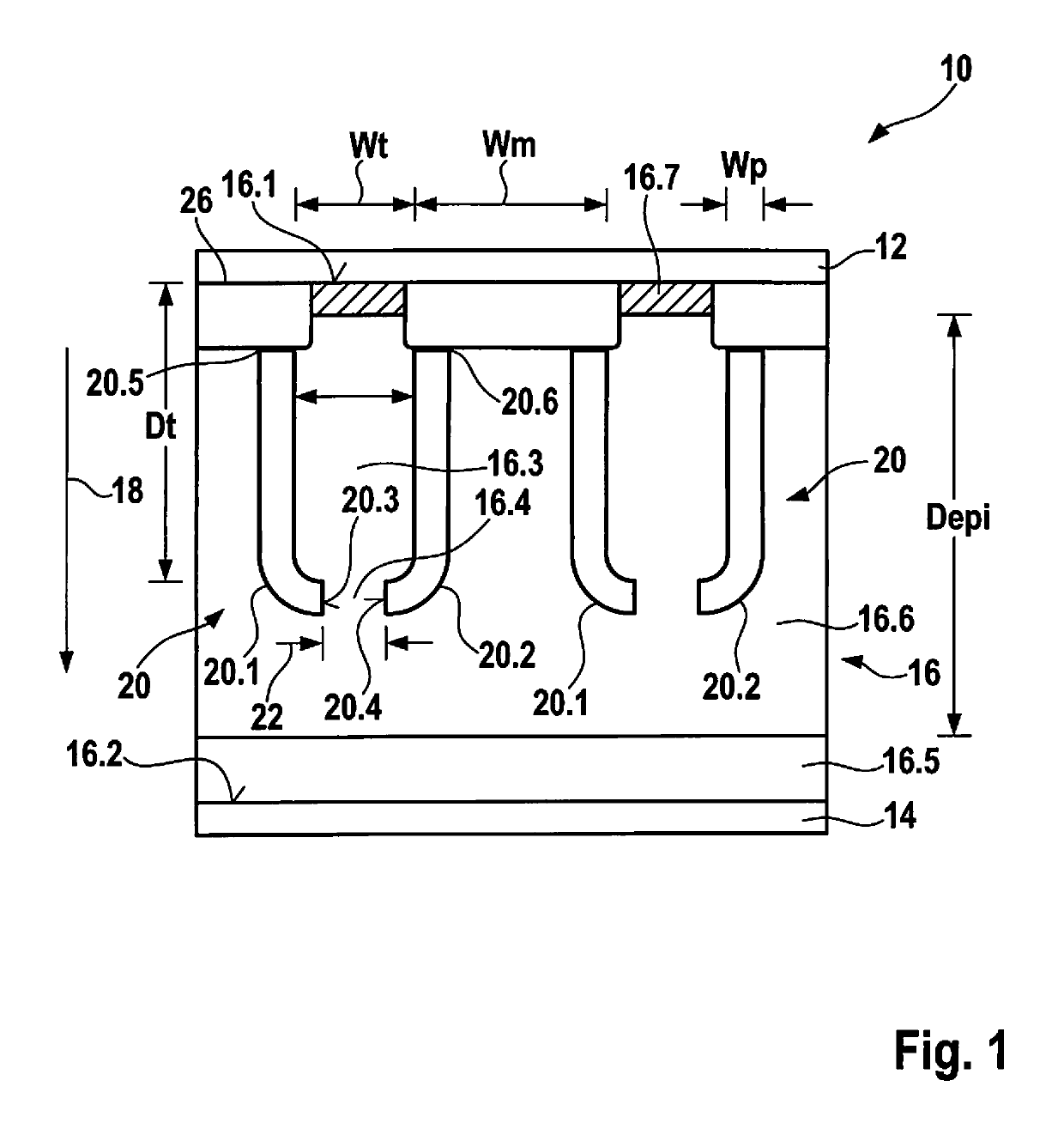
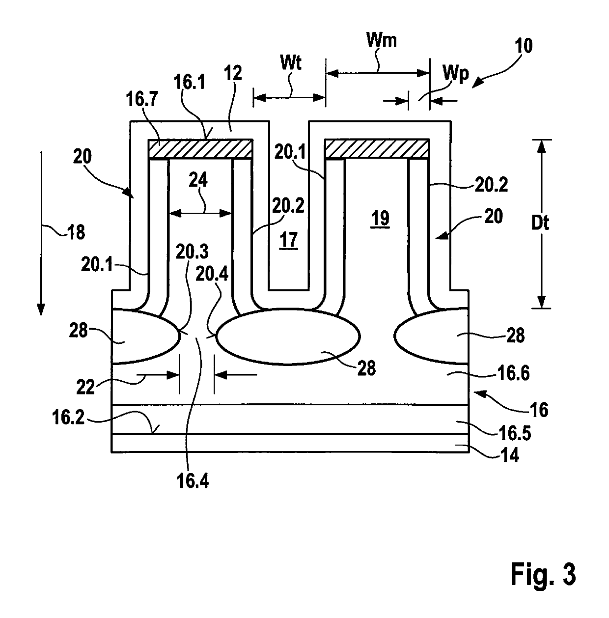
[0019]In detail, FIG. 1 shows a semiconductor system 10 including a planar anode contact 12 and a planar cathode contact 14, and a first volume 16 of n-conductive semiconductor material, which has an anode-side end 16.1 and a cathode-side end 16.2 and extends between planar anode contact 12 and planar cathode contact 14. A direction pointing from anode contact 12 to cathode contact 14 defines a depth direction 18. Semiconductor system 10 has at least one p-conductive area 20 extending from anode-side end 16.1 of first volume 16 in depth direction 18 toward cathode-side end 16.2 of first volume 16 without reaching cathode-side end 16.2 of first volume 16.

[0020]p-conductive area 20 has at least two sub-areas 20.1, 20.2, which are separated from one another, in a cross section lying transversely with respect to anode contact 12 and cathode contact 14, which delimit a first sub-volume 16.3 of first volume 16 filled with the n-conductive semiconductor material, first sub-volume 16. 3 fil...


PUM


Abstract

A semiconductor system including a planar anode contact, a planar cathode contact, and a volume of n-conductive semiconductor material, which has an anode-side end and a cathode-side end and extends between the anode contact and the cathode contact. A p-conductive area extends from the anode-side end of the volume toward the cathode-side end of the volume without reaching the cathode-side end. The p-conductive area has two sub-areas which are separated from one another in a cross section lying transversely with respect to the anode contact and the cathode contact, which delimit a sub-volume of the volume filled with n-conductive semiconductor material. The sub-volume is open toward the cathode contact, and is delimited by cathode-side ends of the sub-areas. A distance of the two sub-areas defining the opening is smaller than a distance between the two sub-areas prevailing outside of the opening and lying between anode side ends of the sub-areas.

Description

CROSS REFERENCE[0001]The present application claims the benefit under 35 U.S.C. § 119 of German Patent Application No. DE 102016204250.5 filed on Mar. 15, 2016, which is expressly incorporated herein by reference in its entirety.BACKGROUND INFORMATION[0002]The present invention relates to a semiconductor system. A conventional semiconductor system includes a planar anode contact and a planar cathode contact and a first volume of n-conductive semiconductor material, which extends between the planar anode contact and the planar cathode contact. A direction pointing from the anode contact to the cathode contact defines a depth direction. The semiconductor system has at least one p-conductive area having an anode-side end and a cathode-side end and which extends from the anode-side end in the depth direction toward the cathode-side end without reaching the cathode-side end.[0003]When alternating current or three-phase current is rectified, alternating current bridges (rectifiers) are us...

Claims


Application Information

Patent Timeline
Patent Type & Authority Patents(United States)
IPC IPC(8): H01L29/06H01L29/861H01L29/66H01L21/02H01L29/47H01L29/16
CPCH01L21/02595H01L29/47H01L29/861H01L29/66136H01L21/02532H01L29/0688H01L29/1608H01L29/16H01L29/66143H01L29/872H01L29/0619H01L29/6609H01L29/0623
Inventor GOERLACH, ALFRED
Owner ROBERT BOSCH GMBH
Why Eureka
Try Eureka