Lateral trench MOSFET

a mosfet and lateral technology, applied in the direction of semiconductor devices, transistors, electrical devices, etc., can solve the problems of deteriorating current flow, insufficient resistance reduction, source layer and drain layer, etc., to achieve small resistance, large connection area, and low resistance

Inactive Publication Date: 2006-01-05
SEIKO INSTR INC
View PDF4 Cites 35 Cited by
  • Summary
  • Abstract
  • Description
  • Claims
  • Application Information

AI Technical Summary

Benefits of technology

[0010] According to the present invention, the semiconductor device including the lateral MOSFET, which has a large connection area between the channel formed in the trench and the source and drain layers and which has a small ON resistance, can be realized without increasing the element area or the number of steps.

Problems solved by technology

However, in the conventional lateral trench MOSFET, the depths of the source layer and the drain layer are shallow with respect to the depth of the trench.
Contact area between the channel and the source and drain layers in the MOSFET is not extended, and thus, the ON resistance is not sufficiently reduced.
Further, it is considerable that the accumulation of the current to one point causes heat generation, which further deteriorates the current flow.
A method of expanding the flow of electrons through the formation of a buried layer etc. may be given in order to effectively use the entire channel, but this method comes with a problem of the increase of the number of manufacturing steps.

Method used


Image

  • Lateral trench MOSFET
  • Lateral trench MOSFET
  • Lateral trench MOSFET

Examples


embodiment 1

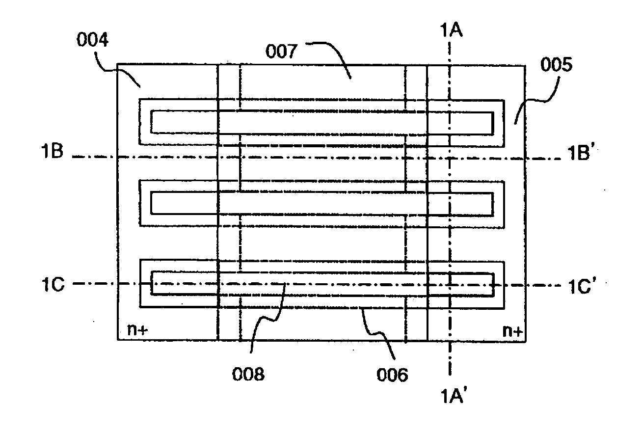
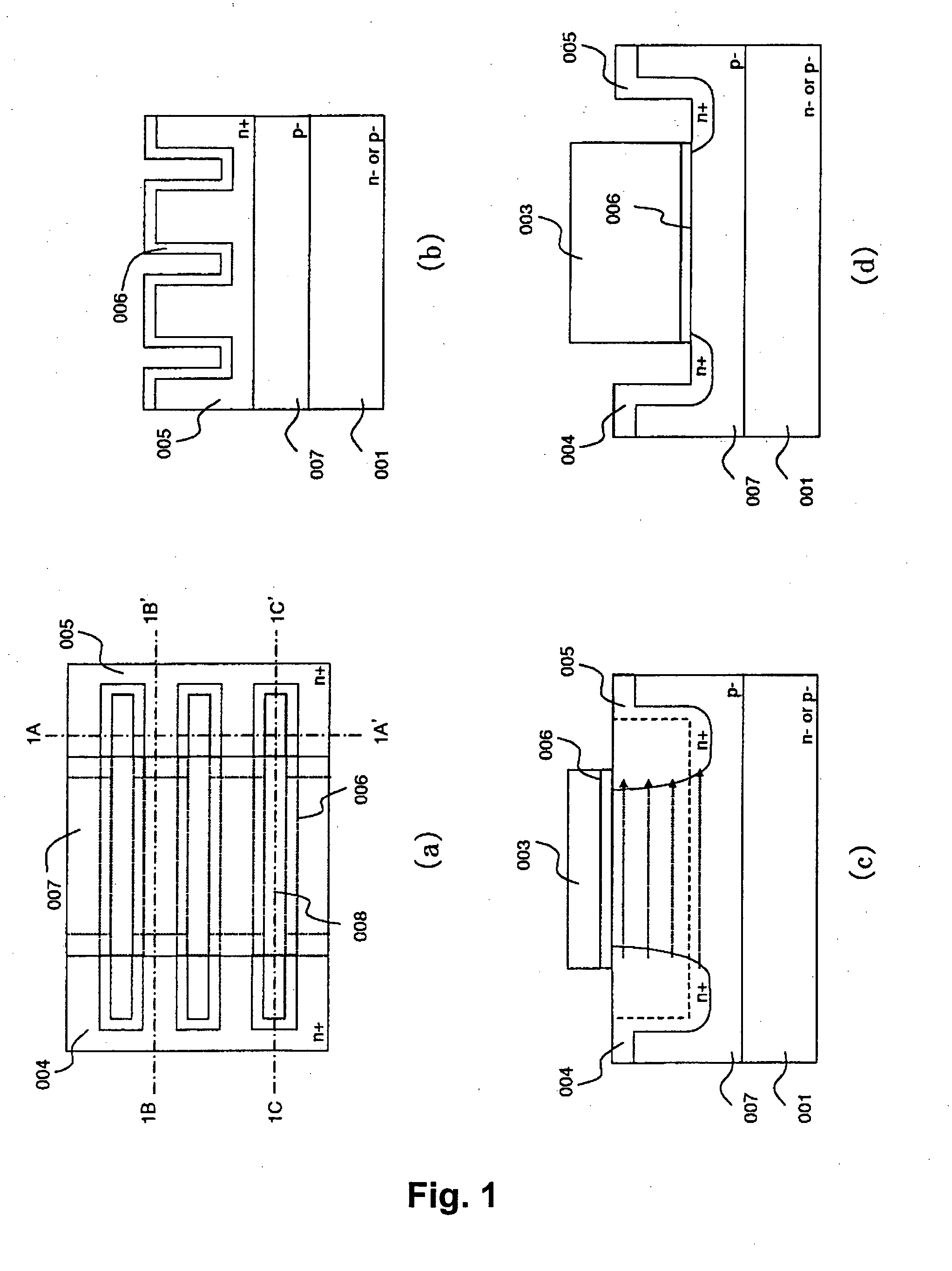
[0018]FIGS. 1A to 1D show Embodiment 1 according to the present invention. FIG. 1A is a plan view, FIG. 1B is a sectional view taken along a line 1A-1A′ in FIG. 1A, FIG. 1C is a sectional view taken along a line 1B-1B′ in FIG. 1A, and FIG. 1D is a sectional view taken along a line 1C-1C′ in FIG. 1A. In this lateral trench MOSFET, a first conductivity type semiconductor layer, for example, a P-type well layer 007 is formed on a high resistance semiconductor substrate 001. Here, the well layer 007 can be omitted by setting an impurity concentration of the semiconductor substrate 001 equal to that of the well layer.

[0019] Plural parallel trenches 008 are formed in the P-type well layer 007 as to reach a point midway in its depth. A gate electrode 003 is formed, through an oxide film 006, on a surface portion of the trench 008 except for the vicinities of both end portions thereof. With the gate electrode 003 as a mask, ion implantation is performed through spinning while holding a cer...

embodiment 2

[0020]FIGS. 3A to 3C show Embodiment 2. FIG. 3A is a plan view, FIG. 3B is a sectional view taken along a line 3A-3A′ in FIG. 3A, and FIG. 3C is a sectional view taken along a line 3B-3B′ in FIG. 3A. This embodiment is a modified structure of Embodiment 1. As shown in FIGS. 3B and 3C, second conductivity type offset layers 009 are formed by using so-calledsidewalls010. With such an offset structure, a higher withstand voltage can be attained in addition to the effects brought by Embodiment 1.

embodiment 3

[0021]FIGS. 4A to 4C show Embodiment 3. FIG. 4A is a plan view, FIG. 4B is a sectional view taken along a line 4A-4A′ in FIG. 4A, and FIG. 4C is a sectional view taken along a line 4B-4B′ in FIG. 4A. This embodiment is a modified structure of Embodiment 1, and includes what is called a DDD (Double Diffused Drain) structure. As shown in FIGS. 4B and 4C, ion implantation is performed only from the drain side and by thermal diffusion a second conductivity type high resistance layer 002 is formed on the drain side. Then ion implantation is performed to both sides to form the source layer 004 and the drain layer 005. This structure can attain a higher withstand voltage in addition to the effects brought by Embodiment 1.


PUM


Abstract

In a lateral trench MOSFET in which a channel width is increased while an element area is not increased to attain reduction in an ON resistance, a source layer (004) and a drain layer (005) are formed in the vicinity of both ends of a trench (008) through multi-directional ion implantation. With this structure, each the source layer (004) and the drain layer (005) are formed deeper than the trench (008), electrons flow through the entire channel region, and an effective channel length becomes shorter. Further reduction of the ON resistance can be realized.

Description

BACKGROUND OF THE INVENTION [0001] 1. Field of the Invention [0002] The present invention relates to a semiconductor device whose ON resistance is low, and more particularly to a semiconductor device provided with a lateral MOSFET. [0003] 2. Description of the Related Art [0004] A lateral MOSFET has been used as a semiconductor switching-device at low voltage. High driving capability is required when a lateral MOSFET is used to switch large current. Reduction of ON resistance is important to improve driving capability. Since resistance of the channel occupies most of the ON resistance of a lateral MOSFET, it is sufficient to increase channel width in order to reduce the ON resistance. [0005] Planer area (hereinafter, referred to as element area) of the lateral MOSFET, however, increases, as the channel width increases. In a conventional lateral trench MOSFET as shown in FIGS. 2A to 2C, plural trenches (grooves) 008 are formed on a substrate surface between a source layer 004 and a d...

Claims


Application Information

Patent Timeline
Patent Type & Authority Applications(United States)
IPC IPC(8): H01L29/76H01L21/336
CPCH01L29/4236H01L29/78H01L29/7835H01L29/7834H01L29/7825
Inventor IGARASHI, ATSUSHI
Owner SEIKO INSTR INC
Why Eureka
Try Eureka