

Photovoltaic cell having discontinuous conductors
- Summary
- Abstract
- Description
- Claims
- Application Information
AI Technical Summary
Benefits of technology
Problems solved by technology
Method used
Image

Examples
first embodiment
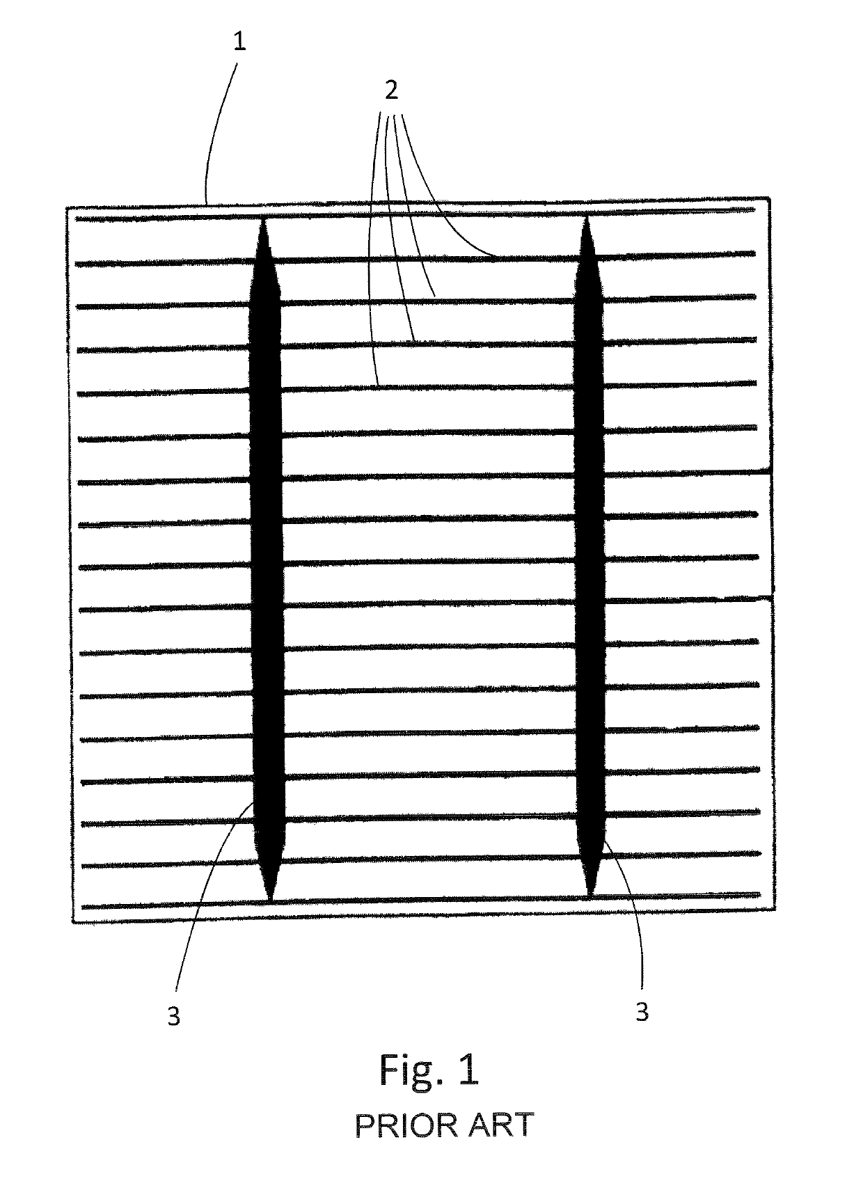
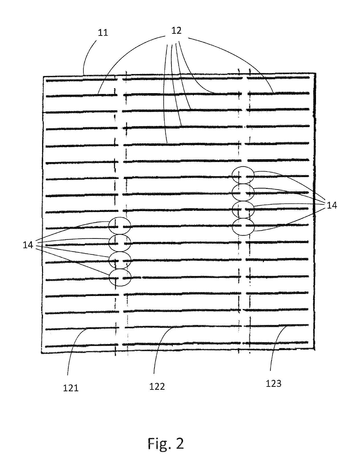
[0035]FIG. 2 shows the invention in which each collecting conductor 12, obtained by stencil printing, is discontinuous, and in fact is made up of three separate segments 121, 122, 123 that are substantially aligned so as to extend across the entire width of the wafer 11. These segments 121, 122, 123 may be 0.07 to 0.12 mm in width, or even less than 0.07 mm in width, about 0.03 to 0.06 mm in width for high-performance cells. This multitude of parallel collecting conductors 12, which form first conductors 12, thus defines what are called interconnection zones 14 in which the conductors 12 are interrupted between two segments 121, 122 and 122, 123. The various interconnection zones 14 of the various collecting conductors 12 are aligned in a different direction to that of the collecting conductors 12, substantially perpendicular to the collecting conductors 12, in order to allow them to be electrically connected using at least one second conductor, for example a copper strip (not shown...
second embodiment
[0049]FIGS. 8 to 10 illustrate a second embodiment in which the conductors 12 are formed in two complementary printing steps using two different stencils. In this particular embodiment, the second printing step fills the voids in the metallization of the first printing step.
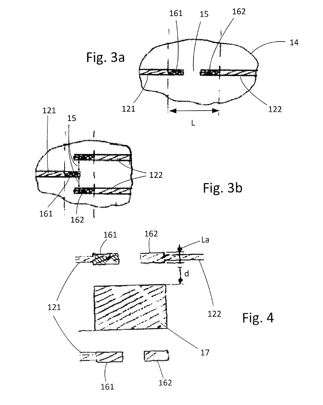
[0050]FIG. 8 thus more precisely shows the geometry obtained in the first printing step using a first stencil, in which printing step the conductor segments 121, 122 produced have mutually facing unconnected wider electrical connectors 161, 162 at their ends. In this embodiment, the electrical connectors have a width La of 0.5 mm and a length of 0.45 mm. They are spaced apart by a gap 15 of 0.45 mm. This first printing step is similar to the printing step carried out in the first embodiment of the invention.
[0051]FIG. 9 shows the imprint produced in the second printing step, which is shifted in the interconnection zone 14 by about 0.45 mm so as to form areas 161′, 162′ in order to produce, finally, a continuous m...
PUM
 Abstract
Description
Claims
Application Information