Electronic device including capacitive structure

a capacitive structure and electronic device technology, applied in the direction of resonance antennas, independent non-interacting antenna combinations, cross-talk/noise/interference reduction, etc., can solve the problems of increasing the length of the wiring line connecting the conductive member and the capacitor, reducing the antenna performance, etc., to reduce the length of the wiring line, and remove the effect of reducing the image curren

Active Publication Date: 2019-11-12
SAMSUNG ELECTRONICS CO LTD
View PDF12 Cites 3 Cited by
  • Summary
  • Abstract
  • Description
  • Claims
  • Application Information

AI Technical Summary

Benefits of technology

[0012]According to various example embodiments of the disclosure, it is possible to remove and / or reduce an image current that deteriorates antenna performance and to reduce the length of a wiring line for ground connection of a PCB by disposing a capacitive structure configured to block a conductive path on a mid-plate.

Problems solved by technology

However, in the above-described conventional electronic device, the number of portions connecting the mid-plate and the PCB through a conductive member is large, and due to this, the length of a wiring line connecting the conductive member and the capacitor is increased.
An increase in the length of the wiring line may cause parasitic resonance, which decreases the performance of the antenna by increasing impedance due to the inductance of the wiring line and the capacitance of the capacitor.

Method used


Image

  • Electronic device including capacitive structure
  • Electronic device including capacitive structure
  • Electronic device including capacitive structure

Examples


Embodiment Construction

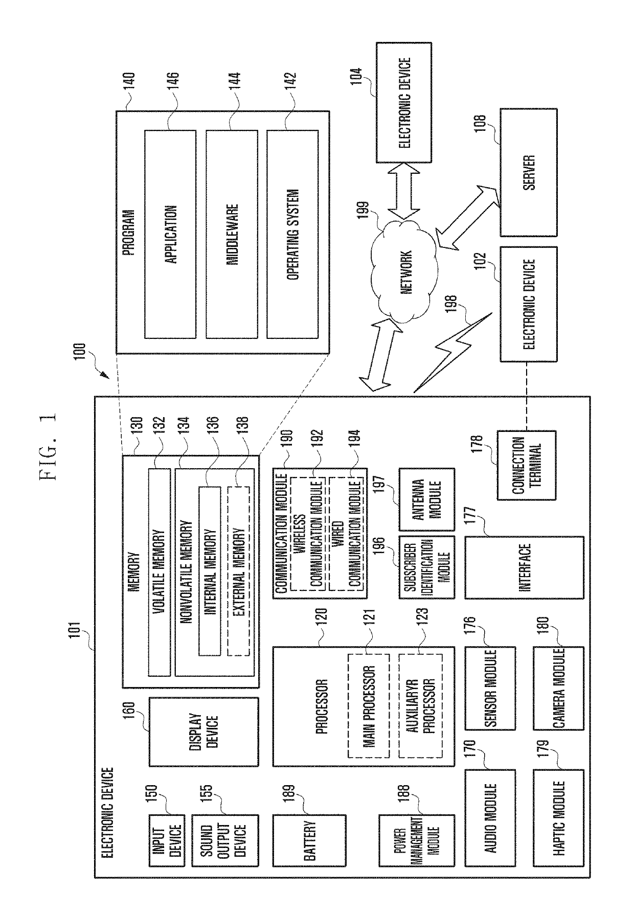
[0030]FIG. 1 is a block diagram illustrating an electronic device 101 in a network environment 100 according to various embodiments. Referring to FIG. 1, the electronic device 101 in the network environment 100 may communicate with an electronic device 102 via a first network 198 (e.g., a short-range wireless communication network), or an electronic device 104 or a server 108 via a second network 199 (e.g., a long-range wireless communication network). According to an embodiment, the electronic device 101 may communicate with the electronic device 104 via the server 108. According to an embodiment, the electronic device 101 may include a processor 120, memory 130, an input device 150, a sound output device 155, a display device 160, an audio module 170, a sensor module 176, an interface 177, a haptic module 179, a camera module 180, a power management module 188, a battery 189, a communication module 190, a subscriber identification module (SIM) 196, or an antenna module 197. In som...


PUM


Abstract

Various embodiments of the disclosure relate to an electronic device including a capacitive structure. The electronic device may include: a housing including a first plate, a second plate facing a direction opposite the first plate, and a side member comprising a side wall surrounding a space between the first plate and the second plate, the side member including a conductive portion; a conductive mid-plate disposed in the housing parallel to the second plate; a dielectric gap formed between the conductive portion and the conductive mid-plate; a printed circuit board (PCB) disposed inside the housing between the conductive mid-plate and the second plate, the PCB including a ground plane; and a capacitive structure comprising a conductive material disposed at a boundary portion of the dielectric gap and the conductive mid-plate between the conductive mid-plate and the PCB, the capacitive structure including a first conductive layer connected to the conductive mid-plate, a second conductive layer spaced apart from the first conductive layer and electrically connected to the ground plane, and a dielectric layer interposed between the first conductive layer and the second conductive layer.

Description

CROSS-REFERENCE TO RELATED APPLICATION[0001]This application is based on and claims priority under 35 U.S.C. § 119 to Korean Patent Application No. 10-2018-0066787, filed on Jun. 11, 2018, in the Korean Intellectual Property Office, the disclosure of which is incorporated by reference herein in its entirety.BACKGROUND1) Field[0002]The disclosure relates to an electronic device including a capacitive structure.2) Description of Related Art[0003]An electronic device may utilize a metal housing exposed to the outside as an antenna. For example, the electronic device may output an RF signal through the antenna, and may generate an electric field by the antenna.[0004]While the electronic device outputs the RF signal through the antenna, an image current corresponding to the electric field generated by the antenna may be induced in a mid-plate disposed in the metal housing to face the antenna. The image current may form an induced electric field when encountering a specific structure insi...

Claims


Application Information

Patent Timeline
Patent Type & Authority Patents(United States)
IPC IPC(8): H05K1/02H01Q1/52H04M1/02H01Q1/48
CPCH01Q1/526H04M1/0277H05K1/0219H01Q1/48H05K1/0231H01Q1/243H01Q9/42H01Q21/28H01Q1/52H05K2201/10371H05K2201/0715H05K2201/10151H05K2201/10121H04M1/026H04B1/40
Inventor KIM, MINSOOJUNG, HYUNTAELEE, JIWOO
Owner SAMSUNG ELECTRONICS CO LTD
Why Eureka
Try Eureka