Memory device with improved latency and operating method thereof

a memory device and latency technology, applied in the field of memory devices, can solve the problems of data loss, fast slow read and write speed of volatile memory devices, such as dynamic random access memory (dram), to achieve the effect of improving read and write speeds

Active Publication Date: 2020-01-14
SAMSUNG ELECTRONICS CO LTD
View PDF22 Cites 0 Cited by
  • Summary
  • Abstract
  • Description
  • Claims
  • Application Information

AI Technical Summary

Benefits of technology

[0006]At least one embodiment of the inventive concept provides a memory device having improved read and write speeds.

Problems solved by technology

The read and write speed of a volatile memory device is fast, but data stored therein is lost when a power supply voltage is interrupted.
In particular, the read and write speeds of the volatile memory device, such as a dynamic random access memory (DRAM), are fast.
However, latency in response time may increase when the capacity of a DRAM is increased too greatly.

Method used


Image

  • Memory device with improved latency and operating method thereof
  • Memory device with improved latency and operating method thereof
  • Memory device with improved latency and operating method thereof

Examples


Embodiment Construction

[0032]Hereinafter, exemplary embodiments of the inventive concept will be described more fully with reference to accompanying drawings. Below, details, such as detailed configurations and structures, are provided to aid a reader in understanding embodiments of the inventive concept. Therefore, embodiments described herein may be variously changed or modified without departing from embodiments of the inventive concept.

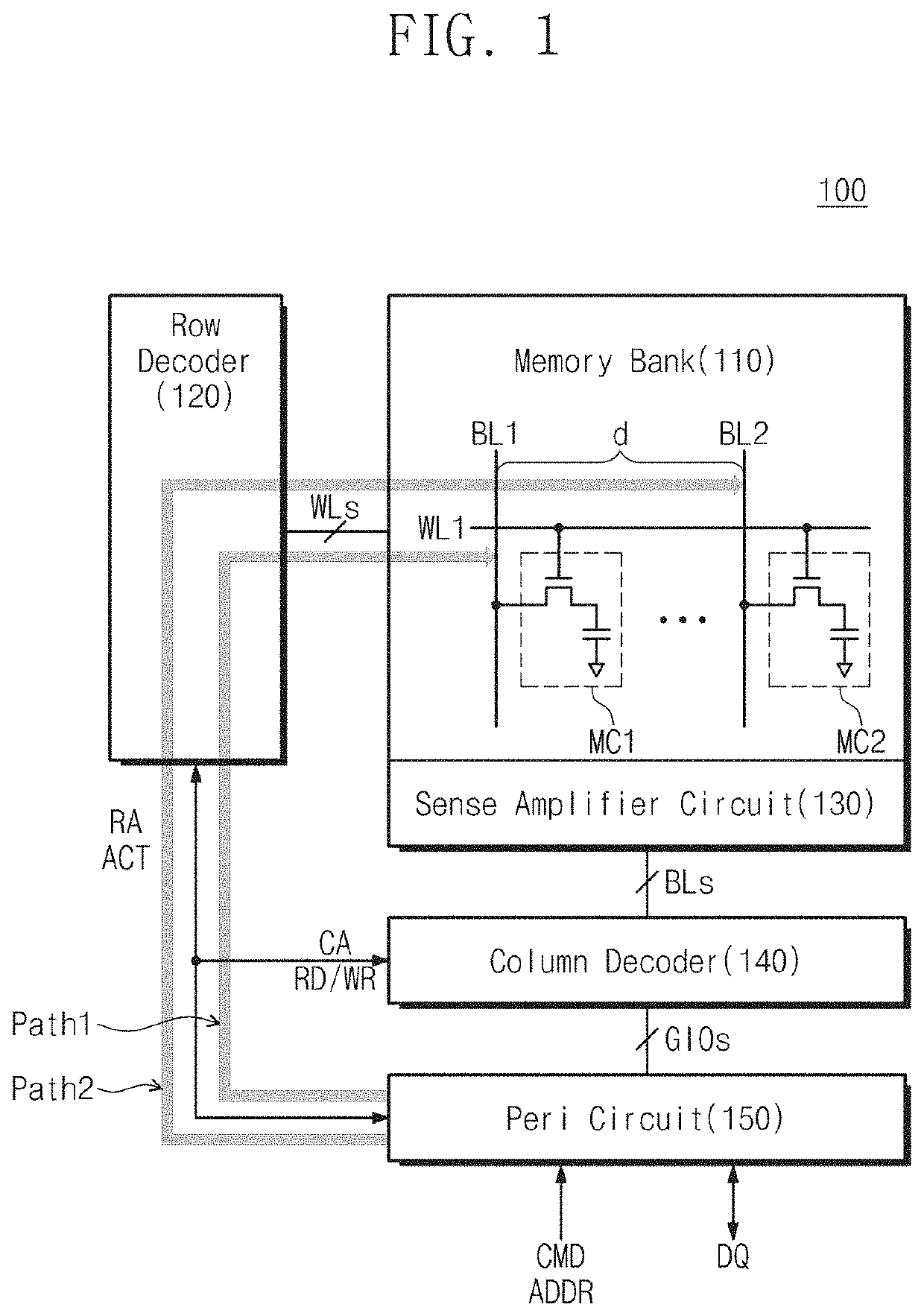
[0033]FIG. 1 is a block diagram illustrating an example of a memory device according to an embodiment of the inventive concept. Referring to FIG. 1, a memory device 100 includes a memory bank 110, a row decoder 120, a sense amplifier circuit 130, a column decoder 140, and a peripheral circuit 150. The sense amplifier circuit 130 may include one or more sense amplifiers.

[0034]The memory bank 110 includes a plurality of memory cells. The memory cells are connected to a plurality of word lines WLs and a plurality of bit lines BLs. For example, the memory cells may be DRAM ...


PUM


Abstract

Disclosed is a memory device which includes a first memory cell connected to a word line and a first bit line, a second memory cell connected to the word line and a second bit line, and a row decoder selecting the word line, a row decoder configured to select the word line, and a column decoder. A first distance between the row decoder and the first memory cell is shorter than a second distance between the row decoder and the second memory cell. The column decoder selects the first bit line based on a time point when the first memory cell is activated.

Description

CROSS REFERENCE TO RELATED APPLICATIONS[0001]This application claims priority under 35 U.S. § 119 to Korean Patent Application No. 10-2016-0076694 filed on Jun. 20, 2016, in the Korean Intellectual Property Office, the disclosure of which is incorporated by reference in its entirety herein.BACKGROUND1. Technical Field[0002]Embodiments of the inventive concept disclosed herein relate to a memory device, and more particularly, to a method of operating a volatile memory device.2. Discussion of Related Art[0003]Semiconductor memory devices are classified into a volatile memory device and a nonvolatile memory device. The read and write speed of a volatile memory device is fast, but data stored therein is lost when a power supply voltage is interrupted. In contrast, a nonvolatile memory device retains data stored therein even when the power supply voltage is interrupted.[0004]In particular, the read and write speeds of the volatile memory device, such as a dynamic random access memory (DR...

Claims


Application Information

Patent Timeline
Patent Type & Authority Patents(United States)
IPC IPC(8): G11C7/00G11C5/06G11C7/10G06F12/02G11C11/408G11C11/4076G11C11/4096G11C11/4093
CPCG06F12/0207G11C11/4087G11C5/063G11C11/4096G11C7/1066G11C7/1093G11C11/4093G11C11/4085G11C11/4076G11C2207/107G06F2212/1024G11C2207/2272G11C8/06G11C8/10G11C11/4082G11C11/4094G11C8/12G11C7/1051
Inventor CHA, SOO-HOKIM, CHANKYUNGPARK, SUNGCHULCHOE, KWANGCHOL
Owner SAMSUNG ELECTRONICS CO LTD
Why Eureka
Try Eureka