

Display device and manufacturing method thereof
a technology of a display device and a manufacturing method, which is applied in the direction of semiconductor devices, instruments, electrical devices, etc., can solve the problems of lithography alignment accuracy, gate electrode accuracy, drain electrode and source electrode accuracy, etc., and achieve the effect of improving the accuracy of lithography alignmen
- Summary
- Abstract
- Description
- Claims
- Application Information
AI Technical Summary
Benefits of technology
Problems solved by technology
Method used
Image

Examples
first embodiment
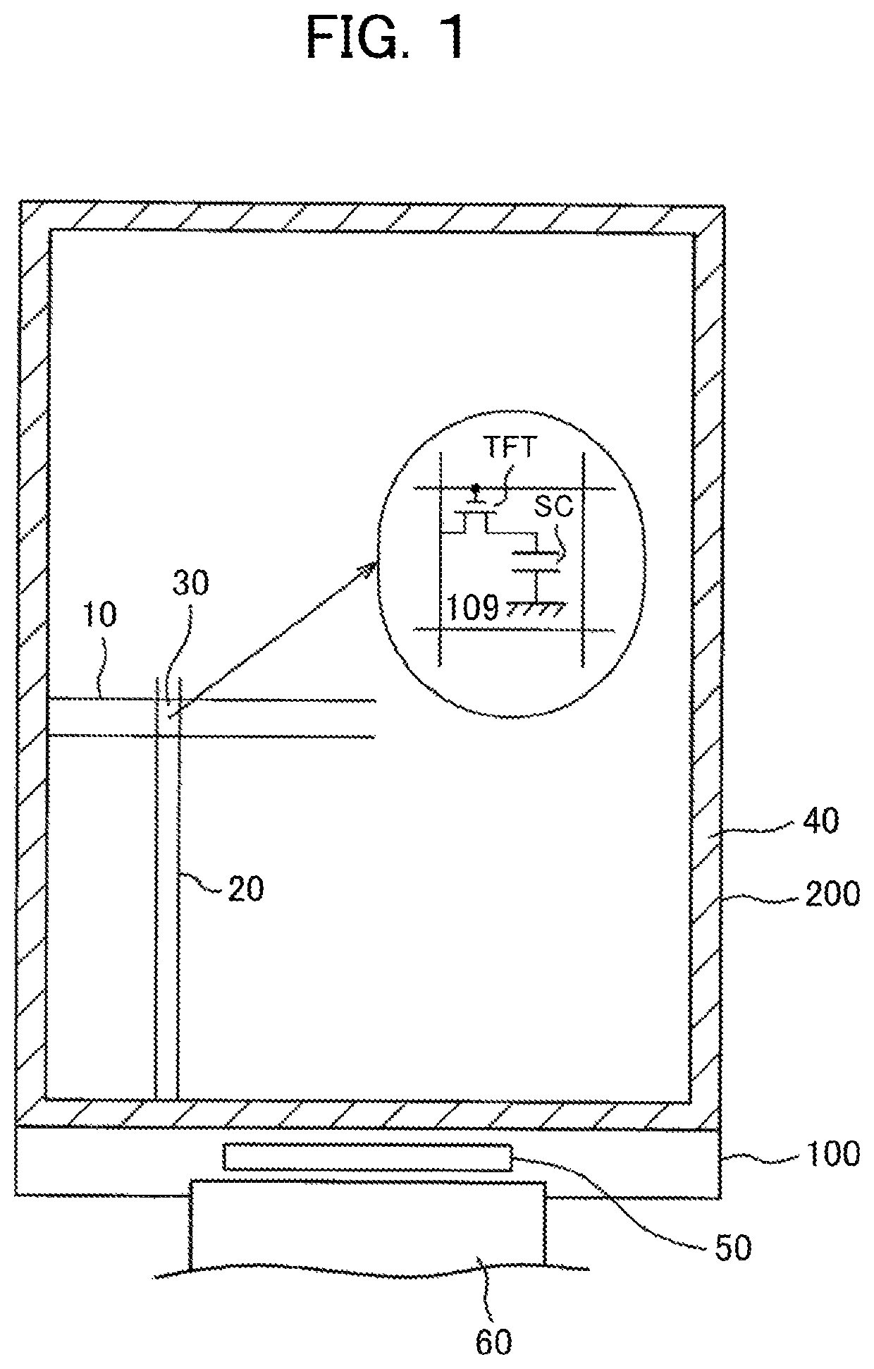
[0036]The invention is explained in regard to the liquid crystal display device, at first. FIG. 1 is a plan view of a liquid crystal display device, which is used in e.g. the cellar phone. In FIG. 1, the TFT substrate 100, in which the scan lines 10 and video signal lines 20 and so on are formed, and the counter substrate 200, in which a black matrix and so on are formed, adhere to each other via the seal material 40. The liquid crystal is sandwiched by the TFT substrate 100 and the counter substrate 200.
[0037]The TFT substrate 100 is bigger than the counter substrate 200; the portion of the TFT substrate 100 that doesn't overlap with the counter substrate 200 is a terminal area. The driver IC 50, which drives the liquid crystal device is installed in the terminal area. The flexible wiring substrate 60, which supplies powers and signals to the liquid crystal display device, is connected to the terminal area.
[0038]In FIG. 1, the scan lines 10 extend in a lateral direction and are arr...
second embodiment
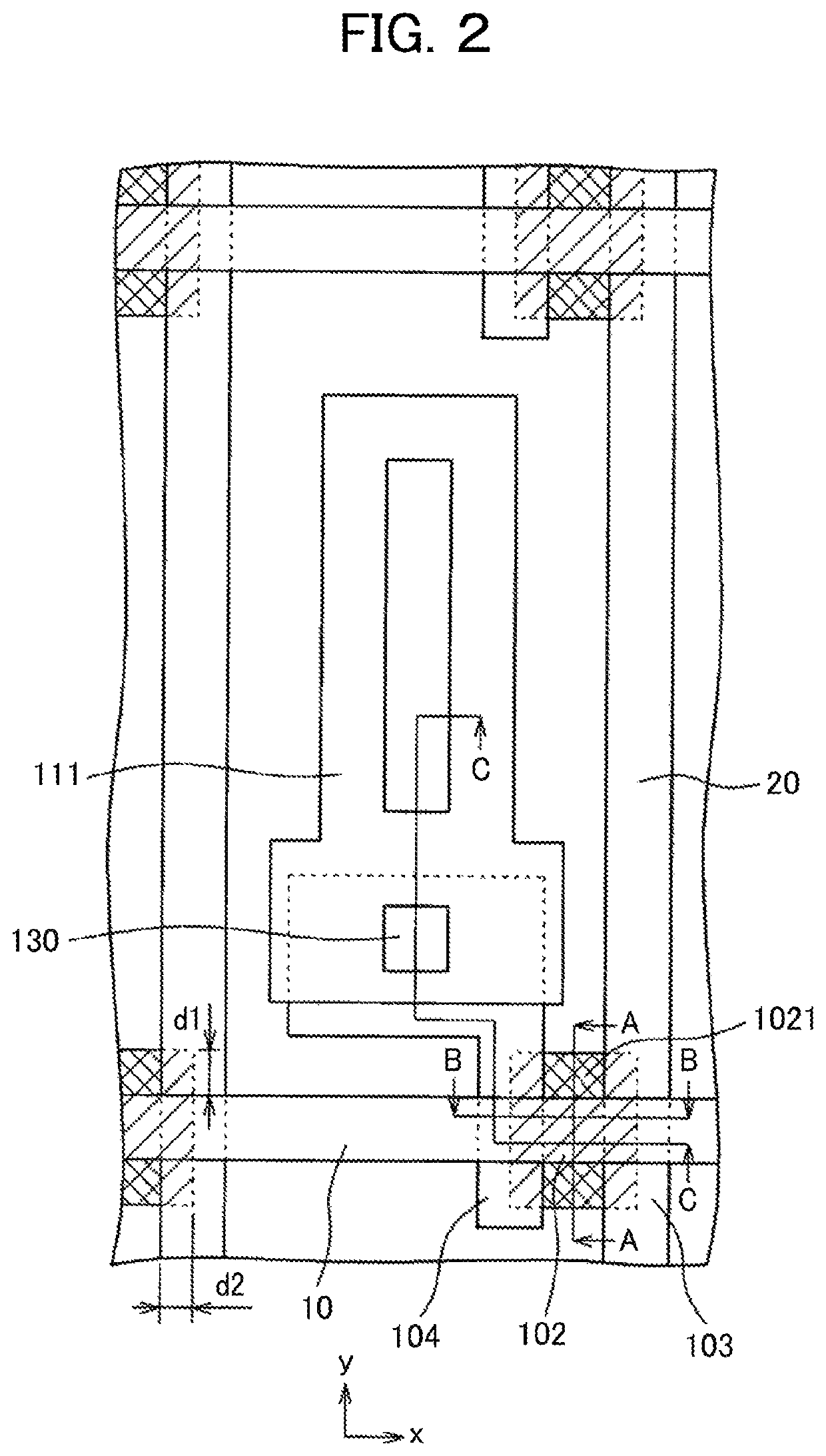
[0059]FIG. 7 is a process flow chart that oxidizes the uncovered area 1021 in FIG. 2 and makes it a high resistance area in the second embodiment. FIG. 7 differs from FIG. 4 in that whole the substrate is exposed to the N2O plasma to oxidize after the gate electrode 106 is patterned. This process is shown by thick frame in FIG. 7. Oxygen supplied from the N2O plasma penetrates the gate insulating film 105 and reaches to the uncovered area 1021 of the oxide semiconductor 102. Consequently, the resistivity of the uncovered area becomes 1 Teraohm·cm or more.
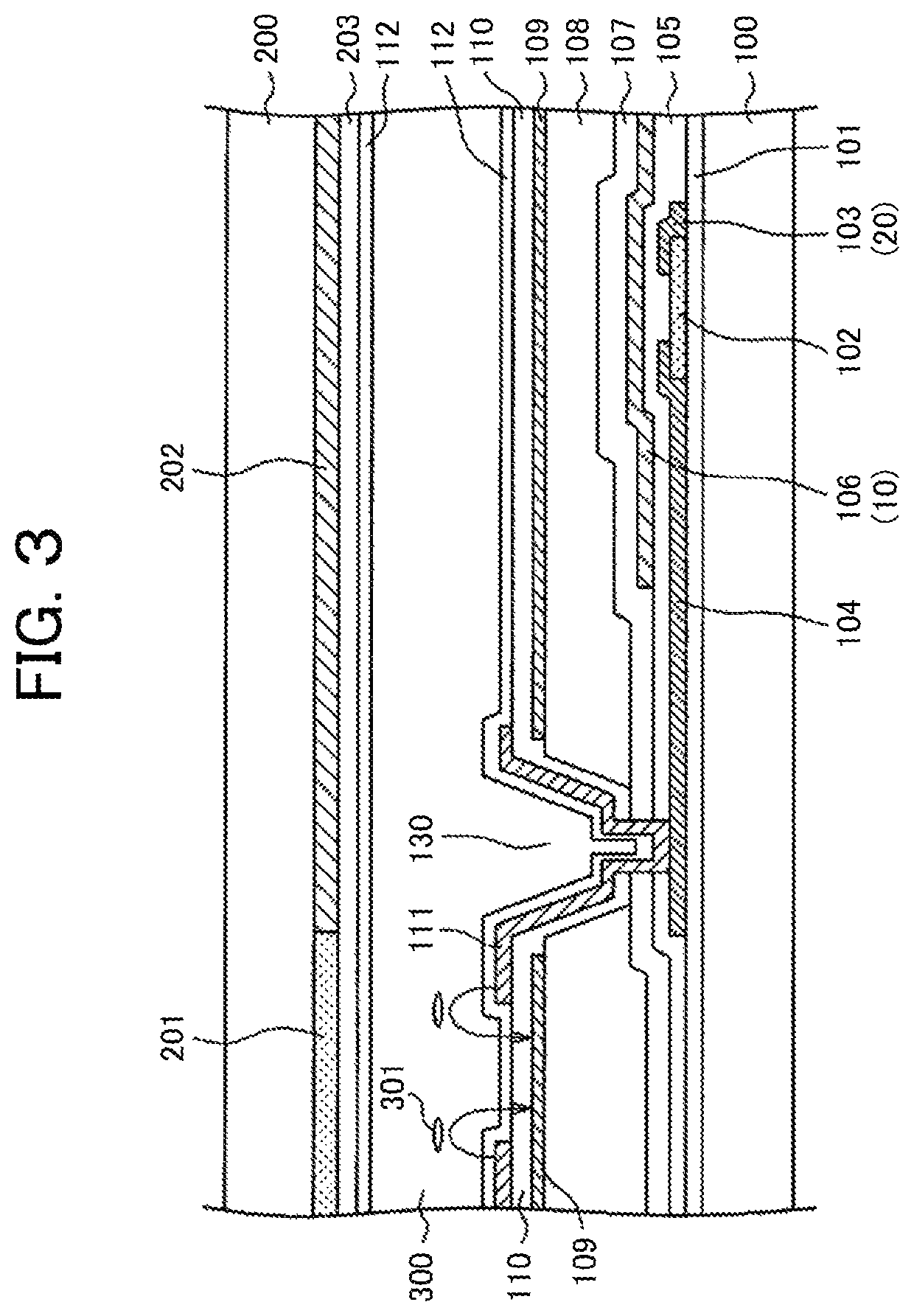
[0060]FIG. 8 is a cross sectional view along the A-A line in FIG. 2. In FIG. 8, oxygen form N2O plasma penetrates the gate insulating film 105 and reaches to the uncovered area 1021; thus, the uncovered area 1021 is oxidized. In the meantime, the area covered by the gate electrode 106 is not oxidized, thus, the characteristics of the channel are not changed. After that, as shown in FIG. 7, the upper layer oxide film 107 is formed by...
third embodiment
[0061]FIG. 9 is a process flow chart that oxidizes the uncovered area 1021 in FIG. 2 and makes it a high resistance area in the third embodiment. FIG. 9 differs from FIG. 4 in that the laser is applied to the oxide semiconductor 102 in an oxygen environment after the gate electrode 106 is patterned to oxidize the uncovered area 1021 of the oxide semiconductor 102. This process is shown by a thick frame in FIG. 9.
[0062]FIG. 10 is a cross sectional view along the A-A line in FIG. 2. When IGZO is chosen as the oxide semiconductor 102, the wave length of the laser is chosen approximately 180 nm to 400 nm so that the laser can efficiently absorbed by IGZO. The laser can be intermittently irradiated with frequency of 250 Hz to 350 Hz. The oxide semiconductor 102 is heated by the laser, consequently, the uncovered area 1021 of the oxide semiconductor 102 easily absorbs oxygen in the oxygen environment; thus, this area is oxidized, consequently, the resistivity of the uncovered area 1021 ca...
PUM
| Property | Measurement | Unit |
|---|---|---|
| resistivity | aaaaa | aaaaa |
| thickness | aaaaa | aaaaa |
| width | aaaaa | aaaaa |
Abstract
Description
Claims
Application Information