
Method for manufacturing a mask

a mask and manufacturing technology, applied in the field of lithography, can solve the problems of bringing certain challenges to masks and their fabrication, computational challenges, and dramatic increases in the write time of such beams, and achieve the effect of efficient and simpl

Active Publication Date: 2020-07-21
INTERUNIVERSITAIR MICRO ELECTRONICS CENT (IMEC VZW) +1
View PDF13 Cites 2 Cited by
  • Summary
  • Abstract
  • Description
  • Claims
  • Application Information

AI Technical Summary

Benefits of technology

[0007]It is an object of the present disclosure to provide an efficient and simple method for manufacturing a mask structure for lithography and a mask structure for lithography manufactured thereof.
[0008]It is an advantage of the embodiments of the present disclosure that feature sizes beyond the resolution of the mask manufacturing process are enabled. This provides maintaining a smaller design volume while not increasing the write-time.
[0009]It is an advantage of the embodiments of the present disclosure that assist features suitable for EUV masks can be manufactured. It is a further advantage of the embodiments of the present disclosure that assist features having sizes less than 8 nm can be manufactured.
[0010]It is a further advantage that the mask data volumes can be significantly smaller.
[0013]It has been realized that using DSA patterning process for the formation of the assist mask feature conveys further the formation of assist features, less than 10 nm for instance, in the absorber layer having smaller sizes, which are beyond the resolution capabilities of the mask manufacturing process. This in turn, can minimize the challenge of increased write-time. Furthermore, since the smaller assist features need not to exist anymore in the mask data, data volume expansion is avoided. Thus, it is an advantage of the embodiments of the present disclosure that the method allows for cost and time efficient manufacturing process for masks for lithography.
[0015]By such a mask structure, the absorber layer may be protected. This can be advantageous since it avoids the contamination or damaging of the absorber layer where one needs to transport the mask structure to another location or to another process tool after provision and phase separation of the BCP material. Contamination or damage on the absorber layer can jeopardize the pattern fidelity on the absorber layer, thus influencing the actual patterns to be made on a substrate. This can adversely affect the device performance.

Problems solved by technology

The switch to heavily-OPCed patterns is computationally challenging, but also brings certain challenges for masks and their fabrication.
Adding the small features forces the e-beam patterning systems to generate very small e-beam “shots” that dramatically increase write time in such beams.
Complex models must be created and calibrated to design and add such small assist features that can make the mask fabrication process quite cumbersome.

Method used


Image

  • Method for manufacturing a mask
  • Method for manufacturing a mask
  • Method for manufacturing a mask

Examples


Embodiment Construction

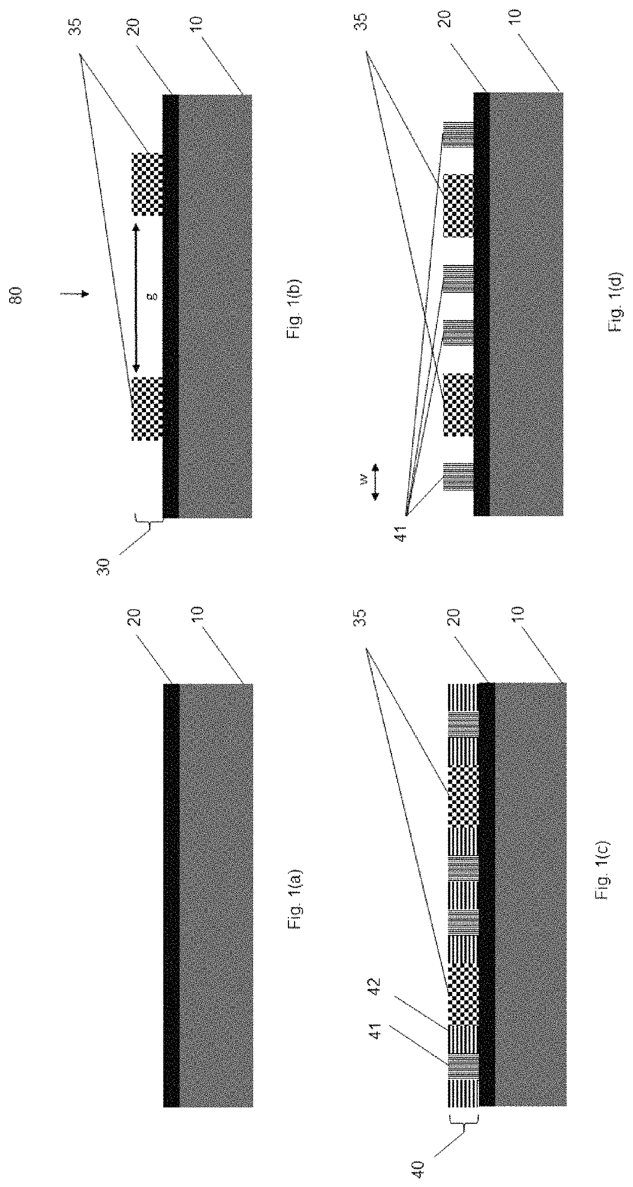
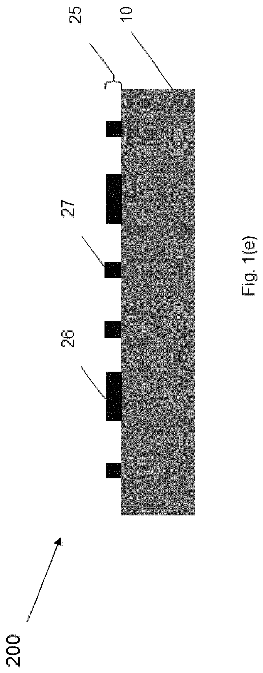
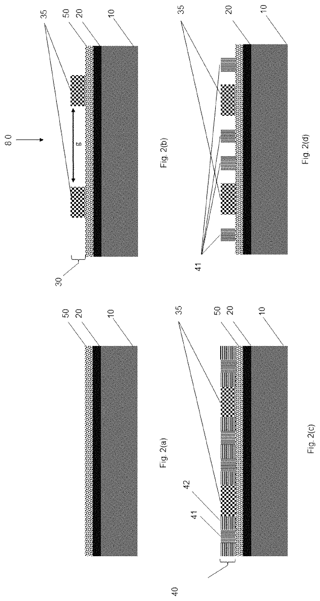
[0023]The present disclosure will be described with respect to particular embodiments and with reference to certain drawings but the disclosure is not limited thereto but only by the claims. The drawings described are only schematic and are non-limiting. In the drawings, the size of some of the elements may be exaggerated and not drawn on scale for illustrative purposes. The dimensions and the relative dimensions do not correspond to actual reductions to practice of the disclosure.

[0024]It is to be noticed that the term “comprising”, used in the claims, should not be interpreted as being restricted to the means listed thereafter; it does not exclude other elements or steps. It is thus to be interpreted as specifying the presence of the stated features, integers, steps or components as referred to, but does not preclude the presence or addition of one or more other features, integers, steps or components, or groups thereof.

[0025]Reference throughout the specification to “one embodime...


PUM

PropertyMeasurementUnit
sizesaaaaaaaaaa
sizesaaaaaaaaaa
phaseaaaaaaaaaa

Abstract

A mask structure and a method for manufacturing a mask structure for a lithography process is provided. The method includes providing a substrate covered with an absorber layer on a side thereof; providing a patterned layer over the absorber layer, the patterned layer comprising at least one opening; and forming at least one assist mask feature in the at least one opening, wherein the at least one assist mask feature is formed by performing a directed self-assembly (DSA) patterning process comprising providing a BCP material in the at least one opening and inducing phase separation of a BCP material into a first component and a second component, the first component being the at least one assist mask feature and being periodically distributed with respect to the second component.

Description

CROSS-REFERENCE TO RELATED APPLICATIONS[0001]This application claims priority from European patent application no. 17189717.6, filed Sep. 6, 2017, which is incorporated by reference in their entirety.TECHNICAL FIELD OF THE DISCLOSURE[0002]The present disclosure is related to the field of lithography. More specifically, it is related to a method for manufacturing a mask.BACKGROUND OF THE DISCLOSURE[0003]In IC manufacturing, lithography is an essential process step. Due to the continuous reduction in feature sizes, optical proximity correction (OPC) techniques are deployed to calculate what photomask pattern should be deployed to create the desired wafer pattern. The switch to heavily-OPCed patterns is computationally challenging, but also brings certain challenges for masks and their fabrication. Therefore, advanced masks should be fabricated to enable the patterning of reduced feature sizes.[0004]In addition to the main design features, sub resolution assist features (SRAF) are typi...

Claims


Application Information

Patent Timeline
Patent Type & Authority Patents(United States)
IPC IPC(8): H01L21/308G03F1/68G03F1/36G03F7/00H01L21/027G03F7/11C09D153/00
CPCG03F1/36G03F1/68H01L21/3086G03F7/0002G03F7/11H01L21/3088H01L21/0274C09D153/005G03F1/38G03F1/54G03F1/76
Inventor GALLAGHER, EMILYGRONHEID, ROELDOISE, JANMOCHI, IACOPO
Owner INTERUNIVERSITAIR MICRO ELECTRONICS CENT (IMEC VZW)
Learn More