
Display device including touch sensing layer

a touch sensing layer and display device technology, applied in the field of display devices, can solve problems such as degradation of display quality, and achieve the effect of minimizing uneven touch sensitivity

Active Publication Date: 2020-08-11
SAMSUNG DISPLAY CO LTD
View PDF13 Cites 2 Cited by
  • Summary
  • Abstract
  • Description
  • Claims
  • Application Information

AI Technical Summary

Benefits of technology

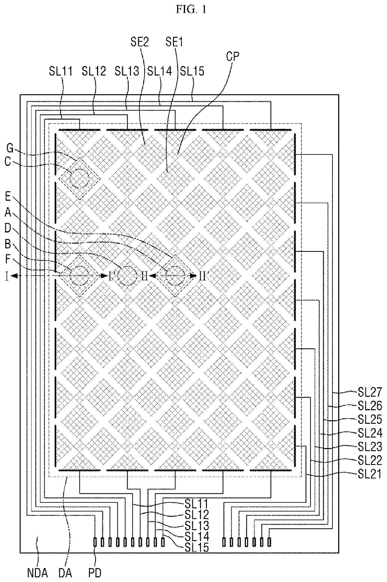
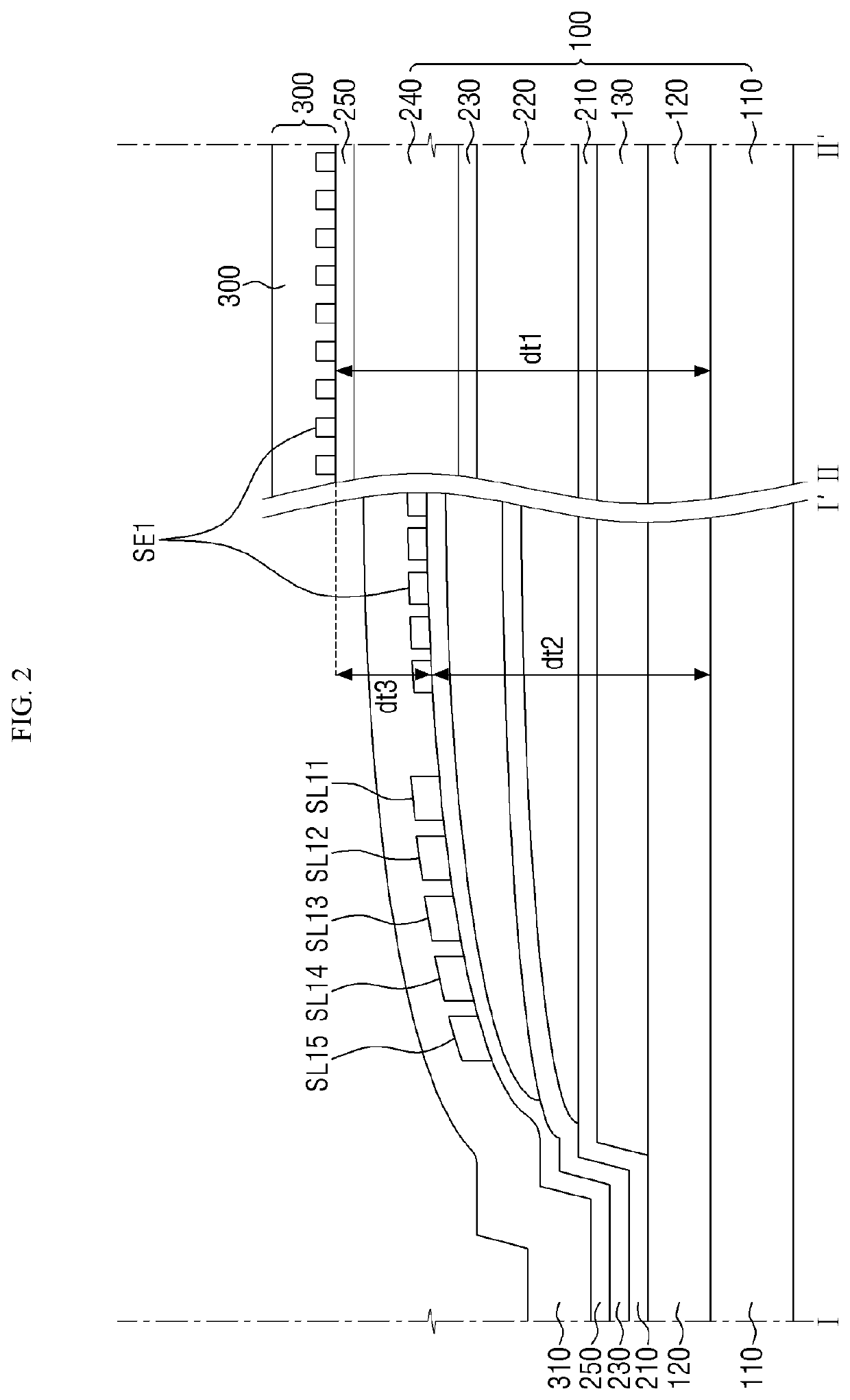
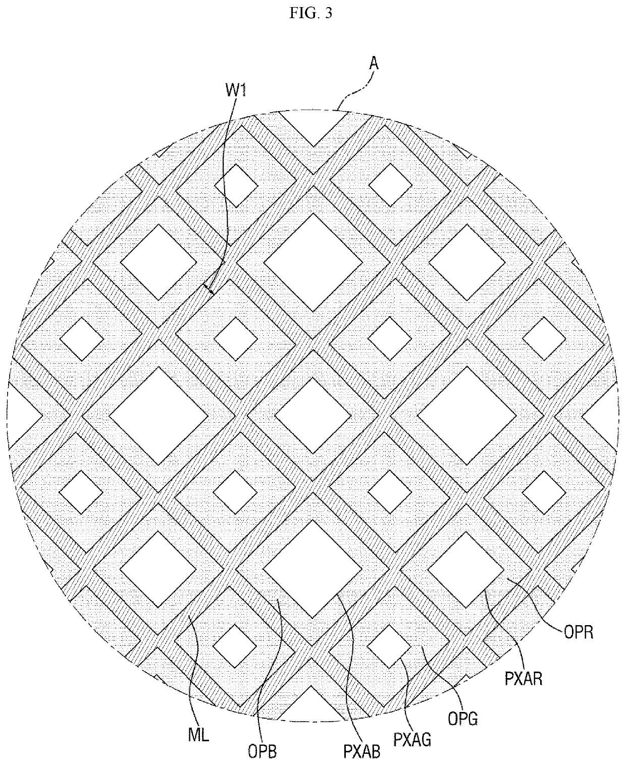
The design ensures uniform touch sensitivity across the display area by adjusting the line widths and patterns of sensing electrodes, compensating for thickness variations in the encapsulation film and reducing noise influence from underlying elements.

Problems solved by technology

Thus, when brought in contact with moisture, oxygen, light, and the like, the electroluminescent unit is highly likely to be damaged and thus to cause degradation of display quality.

Method used


Image

  • Display device including touch sensing layer
  • Display device including touch sensing layer
  • Display device including touch sensing layer

Examples


Embodiment Construction

[0022]The invention will now be described more fully hereinafter with reference to the accompanying drawings, in which embodiments of the invention are shown. This invention may, however, be embodied in different forms and should not be construed as limited to the embodiments set forth herein. Rather, these embodiments are provided so that this disclosure will be thorough and complete, and will fully convey the scope of the invention to those skilled in the art. The same reference numbers indicate the same components throughout the specification. In the attached figures, the thickness of layers and regions is exaggerated for clarity.

[0023]It will be understood that when an element is referred to as being related to another element such as being “on” another element, it can be directly on the other element or intervening elements may be present therebetween. In contrast, when an element is referred to as being related to another element such as being “directly on” another element, th...


PUM

PropertyMeasurementUnit
areaaaaaaaaaaa
widthaaaaaaaaaa
widthsaaaaaaaaaa

Abstract

A display device includes a substrate divided into a display area and a peripheral area, a light-emitting element layer on the substrate and including a light-emitting element, a circuit element layer on the substrate and including a circuit element which drives the light-emitting element, an encapsulation film of which portions thereof are respectively in the display area and the peripheral area, and a plurality of sensing electrodes each on the portion of the encapsulation film which is in the display area, including a plurality of first sensing electrodes and a plurality of second sensing electrodes which intersect the first sensing electrodes. Each of the first sensing electrodes includes a plurality of mesh lines intersecting one another in a mesh shape, and widths of the first sensing electrodes increase as a distance of the first sensing electrode from a center of the display area to the peripheral area decreases.

Description

[0001]This application claims priority to Korean Patent Application No. 10-2017-0097081, filed on Jul. 31, 2017, and all the benefits accruing therefrom under 35 U.S.C. § 119, the disclosure of which is incorporated herein by reference in its entirety.BACKGROUND1. Field[0002]The present disclosure relates to a display device equipped with a touch unit.2. Description of the Related Art[0003]A display device using self-emitting elements, among display devices, has attracted attention as a next-generation display device because of its many advantages such as a fast response speed, capability of realizing a moving image, wide viewing angle, and high luminance.[0004]An electroluminescent unit manufactured using a self-emissive element includes a pixel electrode, an opposing electrode, and an electroluminescent layer interposed between the pixel electrode and the opposing electrode. The electroluminescent unit is highly sensitive to moisture, oxygen, light, and the like. Thus, when brough...

Claims


Application Information

Patent Timeline
Patent Type & Authority Patents(United States)
IPC IPC(8): G06F3/047G06F3/044G06F3/041
CPCG06F3/0418G06F3/0412G06F3/047G06F3/044G06F2203/04112G06F2203/04103G06F3/0446G06F3/04186G06F3/0448G06F3/0443H10K59/40H10K50/805H10K50/84
Inventor LEE, SO LAAN, CHI WOOKJUN, SANG HYUNKIM, JONG SEOKLEE, JAE HYUNJUNG, EUN AE
Owner SAMSUNG DISPLAY CO LTD
Learn More