Structure with micro device having holding structure

a technology of micro-devices and structures, applied in the field of structure with micro-devices, can solve the problems of easy affecting quality of micro-leds and yield rate of delivery, and achieve the effect of improving the yield rate of delivery and transfer of micro-devices

Active Publication Date: 2020-08-18
PLAYNITRIDE
View PDF18 Cites 0 Cited by
  • Summary
  • Abstract
  • Description
  • Claims
  • Application Information

AI Technical Summary

Benefits of technology

[0004]The invention provides a structure with micro device, capable of effectively improving yield rate of delivery and transfer of micro device.
[0006]According to an embodiment of the invention, a horizontal distance between the holding structure and the substrate in a direction parallel to the substrate is gradually increased from the boundary between the top surface and the peripheral surface of the micro device to the substrate.
[0023]According to an embodiment of the invention, a vertical distance between the holding structure and the substrate in a normal direction of the substrate is gradually decreased from the boundary between the top surface and the peripheral surface of the micro device to the substrate.
[0024]Based on the above, in the design of the structure with micro device of the invention, from the cross-sectional view, thickness of the holding structure is not fixed from the boundary between the top surface and the peripheral surface of the micro device to the substrate. With such design, when the micro device is delivered and transferred between different substrates to be applied to, for example, a micro device display, the breaking point of the holding structure can be controlled to be close to the boundary between the top surface and peripheral surface of the micro device, thereby reducing the problem that the holding structure is not completely broken or remained, such that the yield rate of delivery and transfer of the micro LED can be improved.

Problems solved by technology

Typically, the micro LED is held through a holding structure such that the micro LED can be picked up more easily from the carrier as well as delivered and transferred to be placed on the receiving substrate; moreover, the quality of the micro LED is not easily affected by other factors through use of the holding structure to hold the micro LED in the transferring process.
However, the size and shape of a contact area between the holding structure and the micro LED affect the yield rate of delivery and transfer of the micro LED.
In light of the above, it has become an important issue for related industries to find out how to make the holding structure to temporarily hold the micro LED and make the micro LED to be delivered and transferred between the carrier and the receiving substrate more easily and effectively.

Method used


Image

  • Structure with micro device having holding structure
  • Structure with micro device having holding structure
  • Structure with micro device having holding structure

Examples


first embodiment

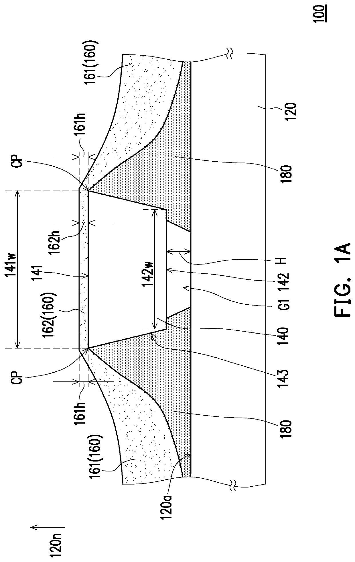
[0046]FIG. 1A is a schematic cross-sectional view of a structure with micro device according to the invention. FIG. 1B is a schematic top view of the structure with micro device in FIG. 1A. Referring to FIG. 1A, a structure with micro device 100 in the embodiment includes a substrate 120, at least one micro device 140, and at least one holding structure 160 and at least one buffering structure 180. The micro device 140 is disposed on the substrate 120 and has a top surface 141 relatively far away from the substrate 120, a bottom surface 142 opposite to the top surface 141 and a peripheral surface 143 connecting the top surface 141 and the bottom surface 142. The holding structure 160 is disposed on the substrate 120. From the cross-sectional view, the thickness of the holding structure 160 in a normal direction 120n of the substrate 120 is gradually increased from a boundary CP between the top surface 141 and the peripheral surface 143 of the micro device 140 to the substrate 120. T...

fifth embodiment

[0060]FIG. 6A is a partial schematic cross-sectional view of a structure with micro device according to another embodiment of the invention. FIG. 6B is a schematic top view of the structure with micro device in FIG. 6A. FIG. 6C is a schematic three-dimensional view of the structure with micro device in FIG. 6A. Referring to FIG. 6A, a structure with micro device 600a of the embodiment is similar to the structure of the micro device 400 of the fifth embodiment, and the difference between the two is that the thickness of the holding structure 660a is not fixed from the boundary between the top surface 641 and the peripheral surface 643a of the micro device 640a to the substrate 620. The micro device 640a is directly connected to the substrate 620 through the holding structure 660a. Specifically, the horizontal distance H1, H2 between the holding structure 660a and the substrate 620 in a direction parallel to the substrate 620 is gradually increased from the boundary between the top su...


PUM

PropertyMeasurementUnit
sizeaaaaaaaaaa
sizeaaaaaaaaaa
vertical distanceaaaaaaaaaa

Abstract

A structure with micro device including a substrate, at least one micro device and at least one holding structure is provided. The micro device is disposed on the substrate and has a top surface away from the substrate, a bottom surface opposite to the top surface, and a circumferential surface connecting the top surface and the bottom surface. The holding structure is disposed on the substrate. From the cross-sectional view, a thickness of the holding structure is not fixed from the boundary of the top surface and the circumferential surface to the substrate. The micro device is connected to the substrate through the holding structure.

Description

CROSS-REFERENCE TO RELATED APPLICATION[0001]This application is a continuation-in-part application of and claims the priority benefit of U.S. application Ser. No. 16 / 212,697, filed on Dec. 7, 2018, now allowed, which claims the priority benefits of U.S. provisional application Ser. No. 62 / 607,325, filed on Dec. 19, 2017, and Taiwan application serial no. 107119254, filed on Jun. 5, 2018. The entirety of each of the above-mentioned patent applications is hereby incorporated by reference herein and made a part of this specification.BACKGROUND OF THE INVENTIONField of the Invention[0002]The invention is related to a semiconductor structure, and particularly to a structure with micro device.Description of Related Art[0003]In current techniques, transfer of micro light emitting diode (LED) is conducted mainly through the means of electrostatic force or magnetic force to transfer the micro LED on a carrier to a receiving substrate. Typically, the micro LED is held through a holding struct...

Claims


Application Information

Patent Timeline
Patent Type & Authority Patents(United States)
IPC IPC(8): H01L33/44H01L21/683H01L33/38
CPCH01L33/44H01L21/6835H01L33/382H01L2221/68368H01L33/54H01L33/56H01L2221/68354
Inventor WU, CHIH-LINGSU, YI-MINLO, YU-YUN
Owner PLAYNITRIDE
Why Eureka
Try Eureka