TFT pixel threshold voltage compensation circuit with short data programming time

a compensation circuit and threshold voltage technology, applied in the field of electronic circuit design and operation, can solve the problems of ultra-short horizontal time, difficult to reduce further without degrading the compensation accuracy, etc., and achieve the effects of reducing power consumption, reducing refresh rate, and increasing initial curren

Active Publication Date: 2020-10-27
SHARP KK
View PDF9 Cites 6 Cited by
  • Summary
  • Abstract
  • Description
  • Claims
  • Application Information

AI Technical Summary

Benefits of technology

[0012]The present invention relates to pixel circuits that are capable of compensating the threshold voltage variations of the drive transistor with an ultra-short one horizontal time 1H of less than about 2 μs, which is shorter as compared to conventional configurations, with additionally shielding the possible data line noise that otherwise is coupled to the gate of the drive transistor in conventional configurations.
[0013]Embodiments of the present application provide pixel circuits for high refresh rate requirements, such as for 120 Hz applications. For such applications, an ultra-short 1H time (<2 μs) is achieved via separation of threshold compensation of the drive transistor and data programming phases. The threshold compensation time is dictated by the drive transistor characteristics and is difficult to reduce further without degrading the compensation accuracy. By separating the threshold compensation and data programming phases, a longer time can be allocated to threshold compensation for compensation accuracy. In addition, as referenced above, the RC constant time required for charging the programming capacitor is determinative of the programming time, and such programming time can be reduced to ultra-short 1H (<2 μs).
[0016]Embodiments of the present application also use an ultra-low leakage oxide transistor, such as an indium gallium zinc oxide (IGZO) transistor, as the data switch device such as transistor T4_2. By using such a device, the stored data voltage is retained longer due to ultra-low leakage of the IGZO transistor. The typical refresh rate is 60 Hz, but with the IGZO transistor the refresh rate can be reduced to 30 Hz or lower for static images. With a lower refresh rate, power consumption can be reduced.
[0017]In addition, during the compensation and programming phases, the EMI signal is applied to the programming capacitor C1. The voltage boost from ΔVEMI through the programming capacitor C1 will make the initial voltage difference between the gate and the source of the drive transistor larger. A larger initial voltage difference will provide a higher initial current to charge the storage capacitor C0, which aids in shortening the threshold compensation time or provides for more accurate threshold compensation. In conventional configurations, the EMI signal is only applied to the emission switch transistor but not to a capacitor that is associated with applying the source voltage to the drive transistor.
[0018]An aspect of the invention, therefore, is a pixel circuit for a display device operable in a compensation phase, a data programming phase, and an emission phase, whereby the one horizontal time is minimized while maintaining accurate compensation of the threshold voltage of the drive transistor, and noise applied to the gate of drive transistor during the emission phase is substantially eliminated. In exemplary embodiments, the pixel circuit includes a drive transistor configured to control an amount of current from a first power supply to a light-emitting device during the emission phase depending upon a voltage input applied to a gate of the drive transistor, and a threshold voltage of the drive transistor is compensated during the compensation phase; wherein the light-emitting device is electrically connected at a first node to a first terminal of the drive transistor during the emission phase and at a second node to a second power supply; a second transistor that is connected between the first power supply and a second terminal of the drive transistor that conducts current from the first power supply to the drive transistor during the emission phase; a first capacitor having a first plate that is connected to the second terminal of the drive transistor and a second plate that is connected to the gate of the drive transistor, and a second capacitor having a first plate that connected to an emission signal input line and a second plate that is connected to the second terminal of the drive transistor and first plate of the first capacitor, wherein the emission signal is applied to the second capacitor during the compensation and data programming phases; and a third transistor and a fourth transistor, wherein the third transistor is connected between a data voltage input line and the fourth transistor, and the fourth transistor is connected between the third transistor and the gate of the drive transistor, such that when the third and the fourth transistors are in an on state during the data programming phase, the data voltage is applied to the gate of the drive transistor. The pixel circuit further may include a fifth transistor that is connected between the first power supply and a node N1 between the third and fourth transistors, such that during the emission phase, the first power supply is applied to the node N1 to shield the drive transistor from noise from the data voltage input line.
[0019]Another aspect of the invention is a method of operating a pixel circuit according to any of the embodiments, whereby the one horizontal time is minimized while maintaining accurate compensation of the threshold voltage of the drive transistor, and noise applied to the gate of drive transistor during the emission phase is substantially eliminated. In exemplary embodiments, the method of operating includes the steps of providing a pixel circuit according to any of the embodiments; performing a compensation phase to compensate a threshold voltage of the drive transistor comprising: electrically disconnecting the second terminal of the drive transistor from the first power supply; boosting the voltage of the second terminal of the drive transistor by applying an emission signal from the emission signal input line to the first plate of the second capacitor; applying a reference voltage from a reference voltage input line to the gate of the drive transistor; and storing the threshold voltage of the drive transistor at the terminals of the first and the second capacitors and the second terminal of the drive transistor; performing a data programming phase to program a data voltage to the capacitors comprising applying the data voltage from the data voltage input line at the first plate of the first capacitor through the third and fourth transistors while the third and fourth transistors are in an on state; and performing an emission phase during which light is emitted from the light-emitting device comprising applying the first power supply through the drive transistor to the light emitting device while the second transistor is in an on state. Performing the emission phase further may include applying the first power supply to the node N1 to shield the drive transistor from noise from the data voltage input line while the fifth transistor is in an on state.

Problems solved by technology

The threshold compensation time is dictated by the drive transistor characteristics and is difficult to reduce further without degrading the compensation accuracy.
The threshold compensation and data programming operations are thus performed independent of each other, which results in an ultra-short one horizontal time due to the short data programming phase.

Method used


Image

  • TFT pixel threshold voltage compensation circuit with short data programming time
  • TFT pixel threshold voltage compensation circuit with short data programming time
  • TFT pixel threshold voltage compensation circuit with short data programming time

Examples


Embodiment Construction

[0027]Embodiments of the present invention will now be described with reference to the drawings, wherein like reference numerals are used to refer to like elements throughout. It will be understood that the figures are not necessarily to scale.

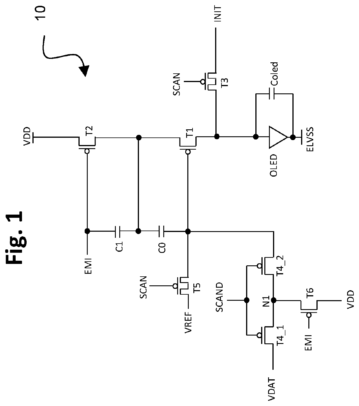
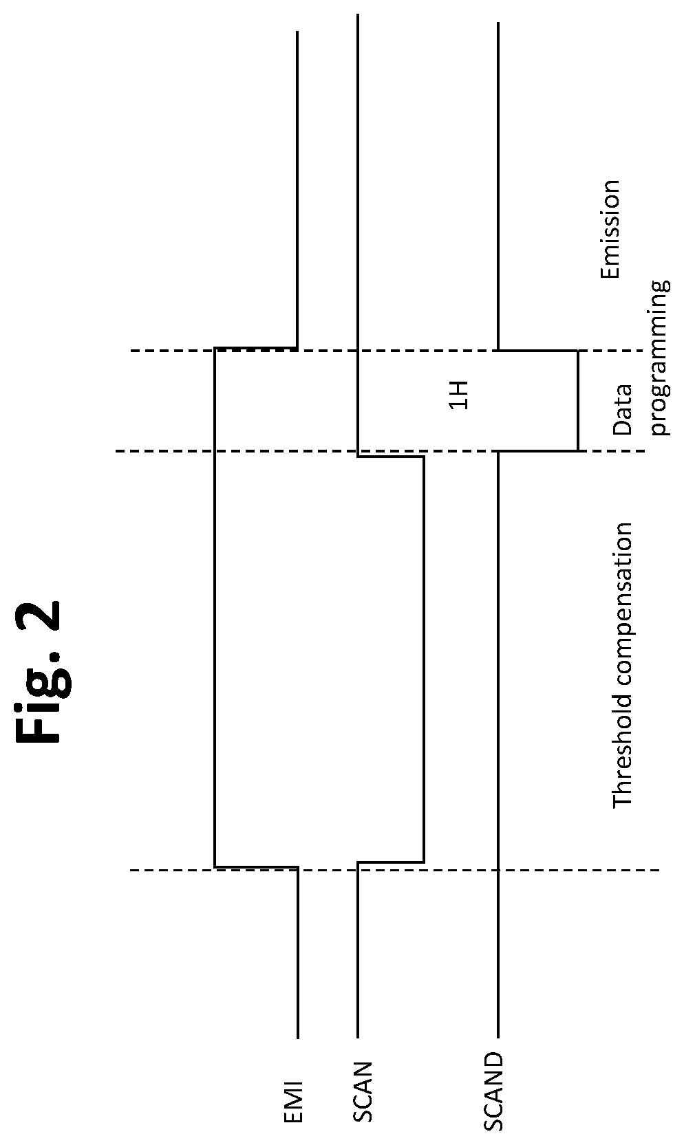
[0028]FIG. 1 is a drawing depicting a first circuit configuration 10 in accordance with embodiments of the present invention, and FIG. 2 is a timing diagram associated with the operation of the circuit configuration 10 of FIG. 1. In this example, the circuit 10 is configured as a TFT circuit that includes multiple p-type transistors T1-T3, T4_1, T4_2, T5, T6 and two capacitors, C0 and C1. In this exemplary embodiment, T3 and T5 are double-gate TFTs as a preferred embodiment, which have low leakage between the source and drain, although T3 and T5 each alternatively may be a single gate TFT. The circuit elements drive a light-emitting device, such as for example an OLED. The light-emitting device (OLED) has an associated internal capacitance, wh...


PUM


Abstract

A pixel circuit for a display device is operable in a compensation phase, a data programming phase, and an emission phase, whereby the one horizontal time is minimized while maintaining accurate compensation of the threshold voltage of the drive transistor, and noise applied to the gate of drive transistor during the emission phase is substantially eliminated. The pixel circuit includes a drive transistor configured to control an amount of current from a power supply to a light-emitting device during the emission phase depending upon a voltage input applied to a gate of the drive transistor, and a threshold voltage of the drive transistor is compensated during the compensation phase. The pixel circuit further includes two transistors, one of which is connected between a data voltage input line and the other transistor, and the other transistor further is connected to the gate of the drive transistor, such that when the two transistors are in an on state during the data programming phase, the data voltage is applied to the gate of the drive transistor. The pixel circuit further may include another transistor that is connected between the power supply and a node N1 between the two transistors, such that during the emission phase, the power supply is applied to the node N1 to shield the drive transistor from noise from the data voltage input line.

Description

TECHNICAL FIELD[0001]The present invention relates to design and operation of electronic circuits for delivering electrical current to an element in a display device, such as for example to an organic light-emitting diode (OLED) in the pixel of an active matrix OLED (AMOLED) display device.BACKGROUND ART[0002]Organic light-emitting diodes (OLED) generate light by re-combination of electrons and holes, and emit light when a bias is applied between the anode and cathode such that an electrical current passes between them. The brightness of the light is related to the amount of the current. If there is no current, there will be no light emission, so OLED technology is a type of technology capable of absolute blacks and achieving almost “infinite” contrast ratio between pixels when used in display applications.[0003]Several approaches are taught in the prior art for pixel thin film transistor (TFT) circuits to deliver current to an element of a display device, such as for example an org...

Claims


Application Information

Patent Timeline
Patent Type & Authority Patents(United States)
IPC IPC(8): G06F3/038G09G5/00G09G3/3291G09G3/3266G09G3/3233G09G5/10
CPCG09G3/3266G09G3/3233G09G3/3291G09G2300/0426G09G2300/043G09G2300/0809G09G2300/0819G09G2300/0852G09G2300/0861G09G2310/021G09G2310/0251
Inventor LU, TONG
Owner SHARP KK
Why Eureka
Try Eureka