Sensor package structure

a technology of package structure and sensor, applied in the direction of semiconductor device details, semiconductor/solid-state device details, radiation control devices, etc., to achieve the effect of improving glare issues

Active Publication Date: 2020-12-15
TONG HSING ELECTRONICS IND LTD
View PDF2 Cites 1 Cited by
  • Summary
  • Abstract
  • Description
  • Claims
  • Application Information

AI Technical Summary

Benefits of technology

[0005]In response to the above-referenced technical inadequacies, the present disclosure provides a sensor package structure to effectively improve the glare issues associated with conventional sensor package structures.
[0007]Therefore, the sensor package structures of the present disclosure are constructed through collocating the light permeable board and the opaque package body (e.g., the first surface is at least partially exposed from the opaque package body, and the inner lateral side of the ring-shaped support is arranged in a projection area formed by orthogonally projecting the platform surface onto the top surface of the sensor chip), the extent the external light signal is reflected by the ring-shaped support after passing through the light permeable board is mitigated, so that the image sensing quality of the sensor chip is improved.

Problems solved by technology

However, some of the external light passing through the light permeable board is reflected by the supporting layer and induces a flare phenomenon, which can easily affect a sensing result of the sensing region.

Method used


Image

  • Sensor package structure
  • Sensor package structure
  • Sensor package structure

Examples


first embodiment

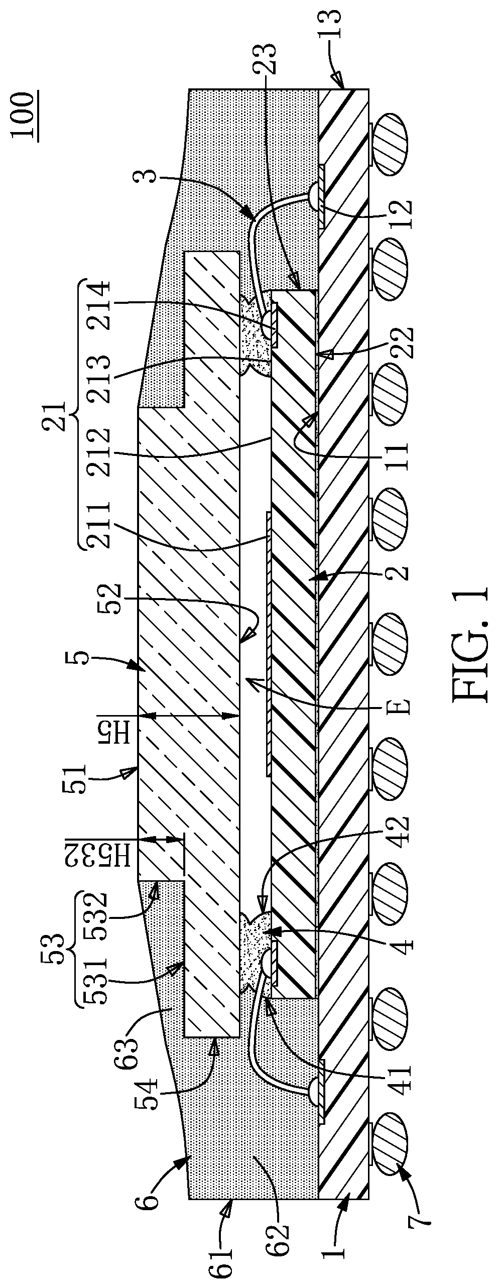
[0013]Referring to FIG. 1, a first embodiment of the present disclosure provides a sensor package structure 100. The sensor package structure 100 includes a substrate 1, a sensor chip 2 disposed on the substrate 1, a plurality of metal wires 3 electrically coupling the substrate 1 and the sensor chip 2, a ring-shaped support 4 disposed on the sensor chip 2, a light permeable board 5 disposed on the ring-shaped support 4, an opaque package body 6 formed on the substrate 1, and a plurality of solder balls 7 disposed on a bottom surface of the substrate 1.

[0014]It should be noted that the drawings of the present embodiment are cross-sectional views for the sake of easily describing the sensor package structure 100 of the present embodiment, and portions of the sensor package structure 100 not shown in the drawings shall have corresponding structures. For example, FIG. 1 shows only two of the metal wires 3 and one row of the solder balls 7, but portions of the sensor package structure 1...

second embodiment

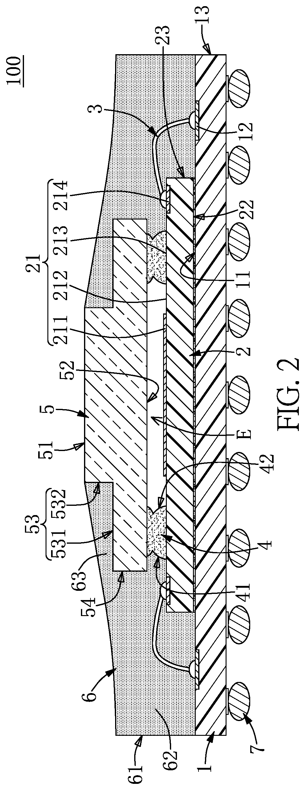
[0025]As shown in FIG. 2, a second embodiment of the present disclosure is provided. The present embodiment is similar to the first embodiment, so identical parts shall not be recited again. The differences between the present and the first embodiment will be described in the following.

[0026]Along the horizontal direction of FIG. 2 of the present embodiment, an outer diameter of the light permeable board 5 is less than that of the sensor chip 2. Moreover, the second pads 214 of the sensor chip 2 are arranged outside of the ring-shaped support 4, so that the metal wires 4 are arranged outside of the ring-shaped support 4 and are entirely embedded in the main portion 62 of the opaque package body 6. According to the first and second embodiments, each of the metal wires 4 of the present disclosure can be at least partially embedded in the main portion 62 of the opaque package body 6.

third embodiment

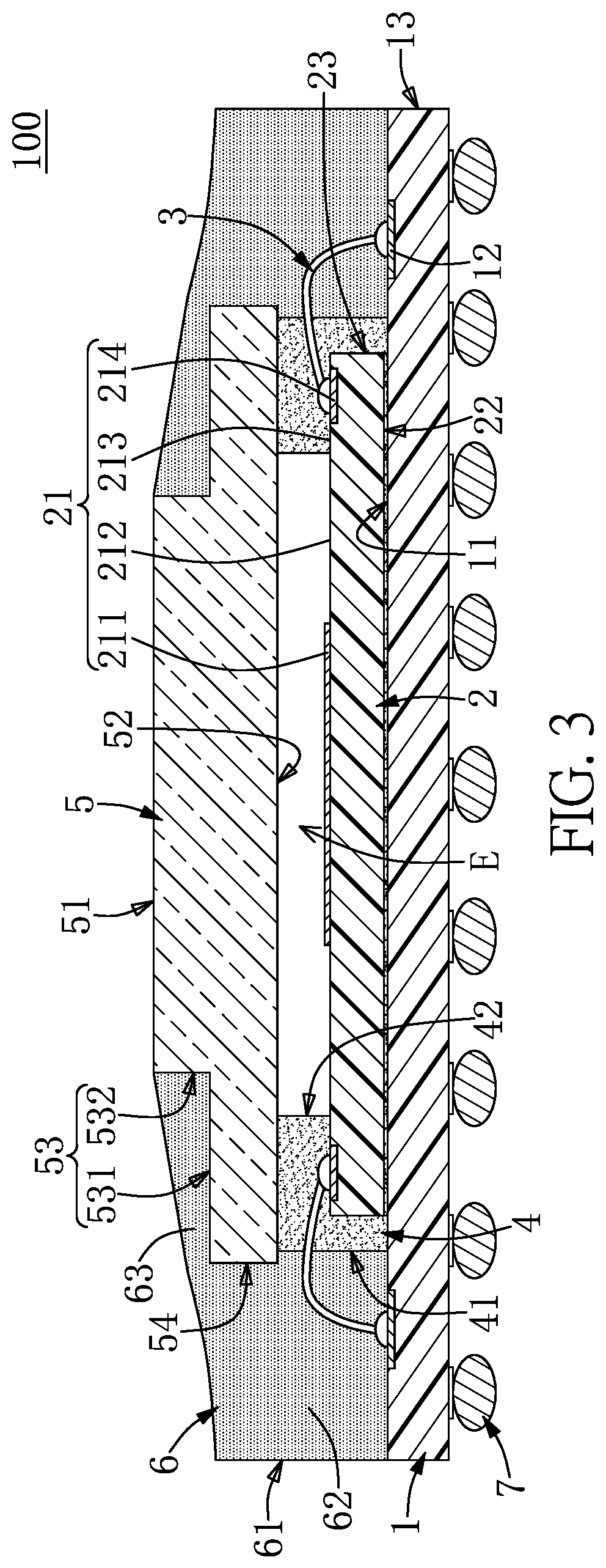
[0027]As shown in FIG. 3, a third embodiment of the present disclosure is provided. The present embodiment is similar to the first embodiment, so identical parts shall not be recited again. The differences between the present and the first embodiment will be described in the following.

[0028]In the present embodiment, the volume of the ring-shaped support 4 is increased to embed a portion of each of the metal wires 3 and further cover the outer lateral side 23 of the sensor chip 2, and the other portion of each of the metal wires 3 is embedded in the main portion 62 of the opaque package body 6.

[0029]In conclusion, the sensor package structures of the present disclosure are constructed through collocating the light permeable board and the opaque package body (e.g., the first surface is at least partially exposed from the opaque package body, and the inner lateral side of the ring-shaped support is arranged in a projection area formed by orthogonally projecting the platform surface on...


PUM

PropertyMeasurementUnit
permeableaaaaaaaaaa
light permeableaaaaaaaaaa
structureaaaaaaaaaa

Abstract

A sensor package structure includes a substrate, a sensor chip on the substrate, a ring-shaped support, a light permeable board on the ring-shaped support, and an opaque package body formed on the substrate. A top surface of the sensor chip includes a spacing region and a carrying region surrounding the spacing region. The support is disposed on the carrying region. The light permeable board has a ring-shaped notch recessed from an upper surface thereof, and the notch includes a platform surface at least partially located above the support and a wall surface connected to the platform surface and located above the spacing region. A portion of the opaque package body fills the notch and is defined as a light shielding portion. An inner lateral side of the support is arranged in a projection area formed by orthogonally projecting the platform surface onto the top surface.

Description

CROSS-REFERENCE TO RELATED PATENT APPLICATION[0001]This application claims priority from the U.S. Provisional Patent Application Ser. No. 62 / 737,357 filed Sep. 27, 2018, which application is incorporated herein by reference in its entirety.[0002]This application claims the benefit of priority to Taiwan Patent Application No. 108113445, filed on Apr. 17, 2019. The entire content of the above identified application is incorporated herein by reference.FIELD OF THE DISCLOSURE[0003]The present disclosure relates to a package structure, and more particularly to a sensor package structure.BACKGROUND OF THE DISCLOSURE[0004]A conventional package structure includes a sensor chip, a light permeable board, and a supporting layer sandwiched between the sensor chip and the light permeable board. A sensing region formed on the top surface of the sensor chip can receive external light passing through the light permeable board. However, some of the external light passing through the light permeable...

Claims


Application Information

Patent Timeline
Patent Type & Authority Patents(United States)
IPC IPC(8): H01L27/146H01L23/00H01L23/04
CPCH01L23/04H01L24/73H01L24/16H01L27/14618H01L27/14636H01L27/14623H01L2224/48091H01L2924/181H01L2224/16225H01L2924/15311H01L2224/73204H01L2924/3025D21H27/10
Inventor LEE, CHIEN-CHENPENG, CHEN-PINLIN, CHIEN-HENGCHEN, JIAN-RU
Owner TONG HSING ELECTRONICS IND LTD
Why Eureka
Try Eureka