
Image sensing device

A technology of image sensing and light sensing, which is applied in the direction of image communication, TV, color TV parts, etc., can solve the problem of reducing the sensing efficiency of image sensing devices, increasing production costs, and being unable to read sensing signals correctly, etc. problem, to achieve the effect of improving image sensing quality

Pending Publication Date: 2021-03-16
EGIS TECH
View PDF0 Cites 0 Cited by
  • Summary
  • Abstract
  • Description
  • Claims
  • Application Information

AI Technical Summary

Problems solved by technology

Although these two methods can improve the problem that the sensing signal cannot be correctly read when the exposure of the sensing pixels is insufficient, they lead to the problem of reducing the sensing efficiency of the image sensing device or increasing the production cost.

Method used


Image

  • Image sensing device
  • Image sensing device
  • Image sensing device

Examples


Embodiment Construction

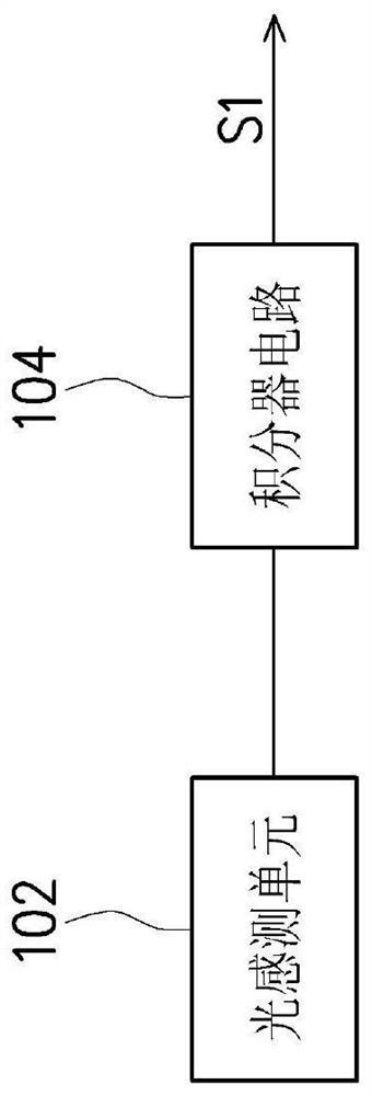
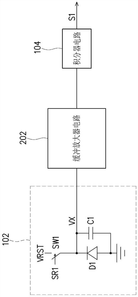
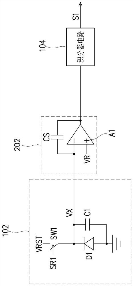
[0014] figure 1 is a schematic diagram of an image sensing device according to an embodiment of the present invention, please refer to figure 1 . The image sensing device may include a light sensing unit 102 and an integrator circuit 104. The light sensing unit 102 is coupled to the integrator circuit 104. The image sensing device may be, for example, a fingerprint sensor or an X-ray flat panel sensor, but it is not limited thereto. . The light sensing unit 102 can receive a light signal including image information to generate a sensing signal. The integrator circuit 104 can perform an integration operation on the sensing signal generated by the light sensing unit 102 during the integration period, so as to accumulate the sensing signal to generate an accumulated sensing value S1 falling within a default range. That is to say, the integrator circuit 104 can continuously sample the sensing signal multiple times during the integration period, and amplify the sensing signal by...


PUM


Abstract

The invention provides an image sensing device. A light sensing unit receives a light signal including image information to generate a sensing signal. An integrator circuit performs integration operation on the sensing signal in an integration period so as to accumulate the sensing signal and generate an accumulated sensing value falling in a default range.

Description

technical field [0001] The invention relates to a sensing device, in particular to an image sensing device. Background technique [0002] A common image sensing device may include a sensing pixel array composed of a plurality of sensing pixels, each sensing pixel may convert incident light into a sensing signal, and by analyzing the sensing signal provided by each sensing pixel, the An image sensed by the image sensing device is obtained. Further, each sensing pixel may include a photodiode, which converts light into an electrical signal. The continuous exposure of the photodiode will cause the voltage value of the sensing signal output by the sensing pixel to continuously decrease. The image sensed by the image sensing device can be obtained by providing the voltage value of the sensing signal. However, when the exposure amount is too small (for example, the exposure time is too short), that is, the voltage value of the sensing signal is too small, the resolution of the r...

Claims


Application Information

Patent Timeline
Patent Type & Authority Applications(China)
IPC IPC(8): H04N5/353
CPCH04N25/53H04N25/77H04N25/78
Inventor 洪自立
Owner EGIS TECH
Learn More