
Ultra-violet light sensing device and manufacturing method thereof

a technology of ultra-violet light and manufacturing method, which is applied in the direction of semiconductor devices, basic electric elements, electrical apparatus, etc., can solve the problems of poor yield rate of multi-layer filter manufacturing process, high cost of multi-layer filter materials, and more loss in manufacturing process, so as to reduce production cost and simplify manufacturing process

Active Publication Date: 2014-12-16
PIXART IMAGING INC
View PDF2 Cites 0 Cited by
  • Summary
  • Abstract
  • Description
  • Claims
  • Application Information

AI Technical Summary

Benefits of technology

The present invention is providing an ultraviolet light sensing device with improved sensing quality for ultraviolet light with a higher signal-to-noise ratio (S / N ratio). This device utilizes a special arrangement of conductivity regions to trap the photoelectrons induced by longer wavelength light and prevent them from interfering with the sensing of ultraviolet light. The device can be manufactured using standard semiconductor processes, reducing production costs and simplifying the manufacturing process.

Problems solved by technology

However, visible light or infrared light can penetrate deeper semiconductor region to induce photoelectrons, and the induced photoelectrons could drift to the shallow semiconductor region which could interfere the sensing result for the ultra-violet light, because both the drifting photoelectrons and the induced photoelectrons are present in the shallow semiconductor region.
However, the yield rate of the multilayer filter manufacturing process is poor.
There is a loss in the deposition process for each layer of the filter, and more number of the layers causes more loss in the manufacturing process.
Further, the material of the multilayer filter is expensive because precious metal like silver is used, so every manufacturing loss will result in a considerable cost.

Method used


Image

  • Ultra-violet light sensing device and manufacturing method thereof
  • Ultra-violet light sensing device and manufacturing method thereof
  • Ultra-violet light sensing device and manufacturing method thereof

Examples


Embodiment Construction

[0025]The drawings as referred to throughout the description of the present invention are for illustration only, but not drawn according to actual scale. The wordings of orientations in the description such as: above, under, left, or right are for reference to the drawings only.

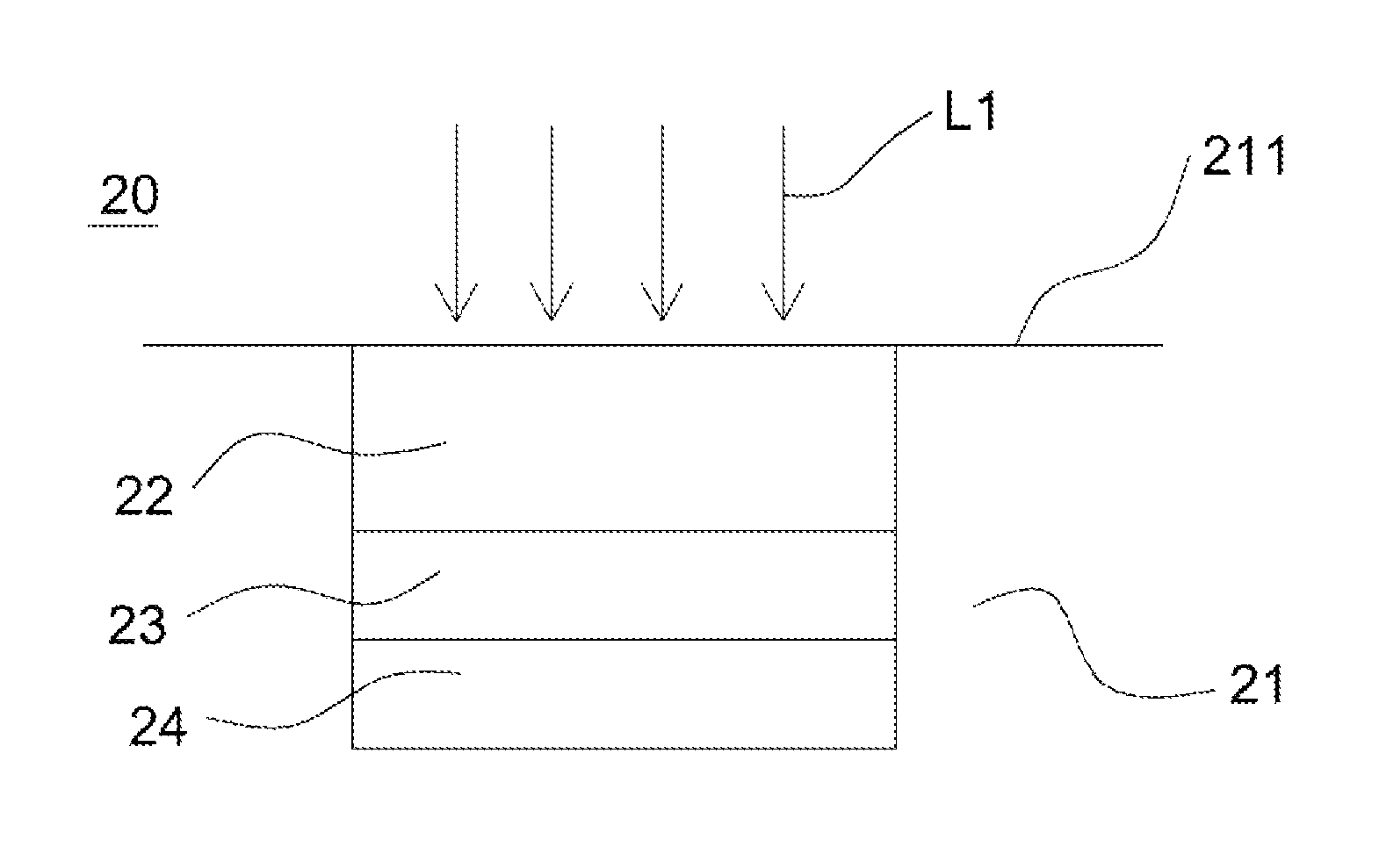
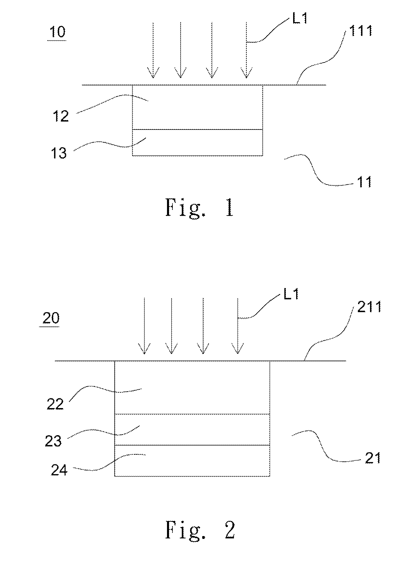
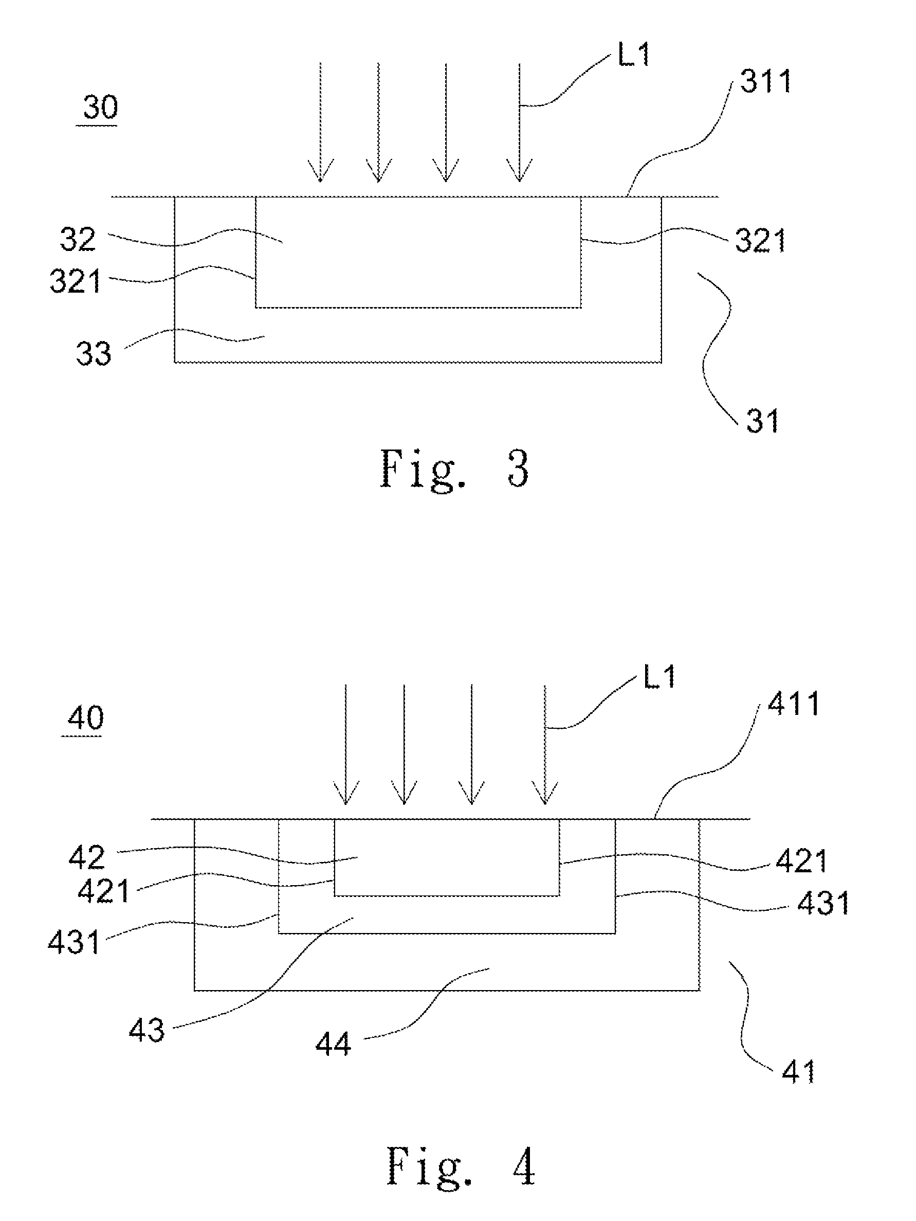
[0026]FIG. 1 shows the cross section view of an embodiment of an ultra-violet light sensing device of the present invention, which can be used for example but not limited in a three-transistor (3T) image sensing circuit (not shown). The ultra-violet light sensing device 10 comprises: a substrate 11 of a first conductivity type, a region 12 of a second conductivity type, and a high density region 13 of the first conductivity type. The high density region 13 has a higher impurity density than the substrate 11. The first conductivity type substrate 11 includes a light incident surface 111 for receiving a light L1. The second conductivity type region 12 is disposed in the first conductivity type substrate 11 and ...


PUM


Abstract

The present invention provides an ultra-violet light sensing device. The ultra-violet light sensing device includes a first conductivity type substrate, a second conductivity type region, and a first conductivity type high density region. The first conductivity type substrate includes a light incident surface. The second conductivity type region is disposed in the first conductivity type substrate and adjacent to the light incident surface. The first conductivity type high density region is disposed under the second conductivity type region. The present invention also provides another ultra-violet light sensing device, which further includes a first conductivity type high density shallow region which is sandwiched between the light incident surface and the second conductivity type region. Manufacturing methods for these ultra-violet light sensing devices are also disclosed in the present invention.

Description

CROSS REFERENCE[0001]The present invention claims priority to TW 101121989, filed on Jun. 20, 2012.BACKGROUND OF THE INVENTION[0002]1. Field of Invention[0003]The present invention relates to an ultra-violet light sensing device, especially an ultra-violet light sensing device with high signal / noise (S / N) ratio.[0004]2. Description of Related Art[0005]Traditional semiconductor based light sensing devices like photo diode are usually used for sensing visible light or infrared light. As for the ultra-violet light, because of its shorter wavelength band (0 nm˜400 nm), the ultra-violet light can only penetrate shallow semiconductor region to induce photoelectrons. However, visible light or infrared light can penetrate deeper semiconductor region to induce photoelectrons, and the induced photoelectrons could drift to the shallow semiconductor region which could interfere the sensing result for the ultra-violet light, because both the drifting photoelectrons and the induced photoelectrons...

Claims


Application Information

Patent Timeline
IPC IPC(8): H01L21/00H01L31/0248H01L33/00
CPCH01L31/0248H01L31/103H01L31/03529Y02E10/50
Inventor LIU, HAN-CHIPAN, HUAN-KUNOKAMOTO, EIICHI
Owner PIXART IMAGING INC
Learn More