Supercharge Your Innovation With Domain-Expert AI Agents!

Leadless semiconductor package with wettable flanks

a technology of leadless semiconductors and flanks, which is applied in the direction of semiconductor devices, semiconductor/solid-state device details, electrical apparatus, etc., can solve the problems of not being suitable for high-reliability applications, solder joints are not easily detected by aoi systems, and current leadless packages are easy to be detected. , to achieve the effect of preventing oxidation, and improving the formation of solder fillets

Active Publication Date: 2021-07-20
STMICROELECTRONICS SRL
View PDF4 Cites 0 Cited by
  • Summary
  • Abstract
  • Description
  • Claims
  • Application Information

AI Technical Summary

Benefits of technology

This solution enables the formation of solder fillets that extend outward from the package, allowing for easy detection by inspection systems, thereby making the packages suitable for high reliability applications by ensuring proper electrical connections.

Problems solved by technology

Unfortunately, solder joints for many current leadless packages are not consistently formed such that the solder joints may be easily detected by AOI systems.
Consequently, the solder joints are not easily detected by AOI systems.
Accordingly, current leadless packages are not suitable for high reliability applications in which solder joints should be checked by inspection systems, such as AOI systems, for proper electrical connections.

Method used


Image

  • Leadless semiconductor package with wettable flanks
  • Leadless semiconductor package with wettable flanks
  • Leadless semiconductor package with wettable flanks

Examples


Embodiment Construction

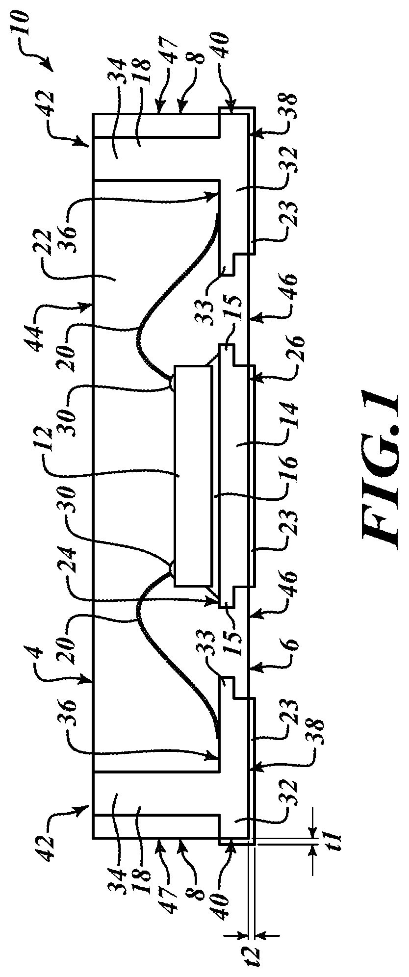
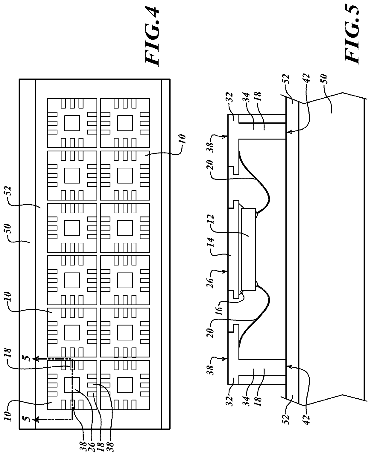
[0014]In the following description, certain specific details are set forth in order to provide a thorough understanding of various aspects of the disclosed subject matter. However, the disclosed subject matter may be practiced without these specific details. In some instances, well-known structures and methods of manufacturing electronic devices have not been described in detail to avoid obscuring the descriptions of other aspects of the present disclosure.

[0015]Unless the context requires otherwise, throughout the specification and claims that follow, the word “comprise” and variations thereof, such as “comprises” and “comprising,” are to be construed in an open, inclusive sense, that is, as “including, but not limited to.”

[0016]Reference throughout the specification to “one embodiment” or “an embodiment” means that a particular feature, structure, or characteristic described in connection with the embodiment is included in at least one embodiment. Thus, the appearance of the phras...


PUM

PropertyMeasurementUnit
thicknessaaaaaaaaaa
thicknessaaaaaaaaaa
thickness t2aaaaaaaaaa

Abstract

The present disclosure is directed to leadless semiconductor packages with improved wettable flanks that encourage the formation of solder fillets when the leadless semiconductor package is mounted to a substrate. The solder fillets are consistently formed and are easily detectable by inspection systems, such as automated optical inspection (AOI) systems.

Description

BACKGROUNDTechnical Field[0001]The present disclosure is directed to a leadless semiconductor package and a method for making the same.Description of the Related Art[0002]A leadless package is a semiconductor package that encapsulates one or more integrated circuits. Leadless packages have near chip scale footprints and thin profiles compared to other types of packages, and, thus, are commonly used for applications in which small packages are desired.[0003]In contrast to a leaded package, a leadless package is not mounted to a substrate, such as a printed circuit board (PCB), by inserting metal legs in to through holes in the substrate. Rather, a leadless package includes leads (sometimes referred to as lands) that are exposed on a bottom surface and / or side surfaces of the leadless package, and is mounted to a substrate using surface mount technology (SMT). For example, a common method to mount a leadless package to a PCB is to solder the leads to contact pads on the PCB.[0004]Once...

Claims


Application Information

Patent Timeline
Patent Type & Authority Patents(United States)
IPC IPC(8): H01L23/495H01L23/00H01L23/31H01L21/48H01L21/56
CPCH01L23/49541H01L23/3121H01L23/49503H01L23/49513H01L23/49575H01L24/45H01L24/48H01L21/4821H01L21/561H01L21/565H01L24/32H01L24/73H01L24/83H01L24/85H01L24/92H01L24/97H01L2224/32245H01L2224/48091H01L2224/48106H01L2224/48245H01L2224/73265H01L2224/92247H01L2924/181H01L23/49548H01L23/49582H01L21/4828H01L2224/48247H01L2224/2919H01L24/29H01L2224/97H01L2924/00012H01L2924/00014H01L2224/83H01L2224/85H01L2924/00
Inventor ARELLANO, IAN HARVEYCADAG, AARONCADAG, ELA MIA
Owner STMICROELECTRONICS SRL
Features
  • R&D
  • Intellectual Property
  • Life Sciences
  • Materials
  • Tech Scout
  • Unparalleled Data Quality
  • Higher Quality Content
  • 60% Fewer Hallucinations
Learn More