Semiconductor package molding device and method of manufacturing semiconductor device
- Summary
- Abstract
- Description
- Claims
- Application Information
AI Technical Summary
Benefits of technology
Problems solved by technology
Method used
Image

Examples
Embodiment Construction
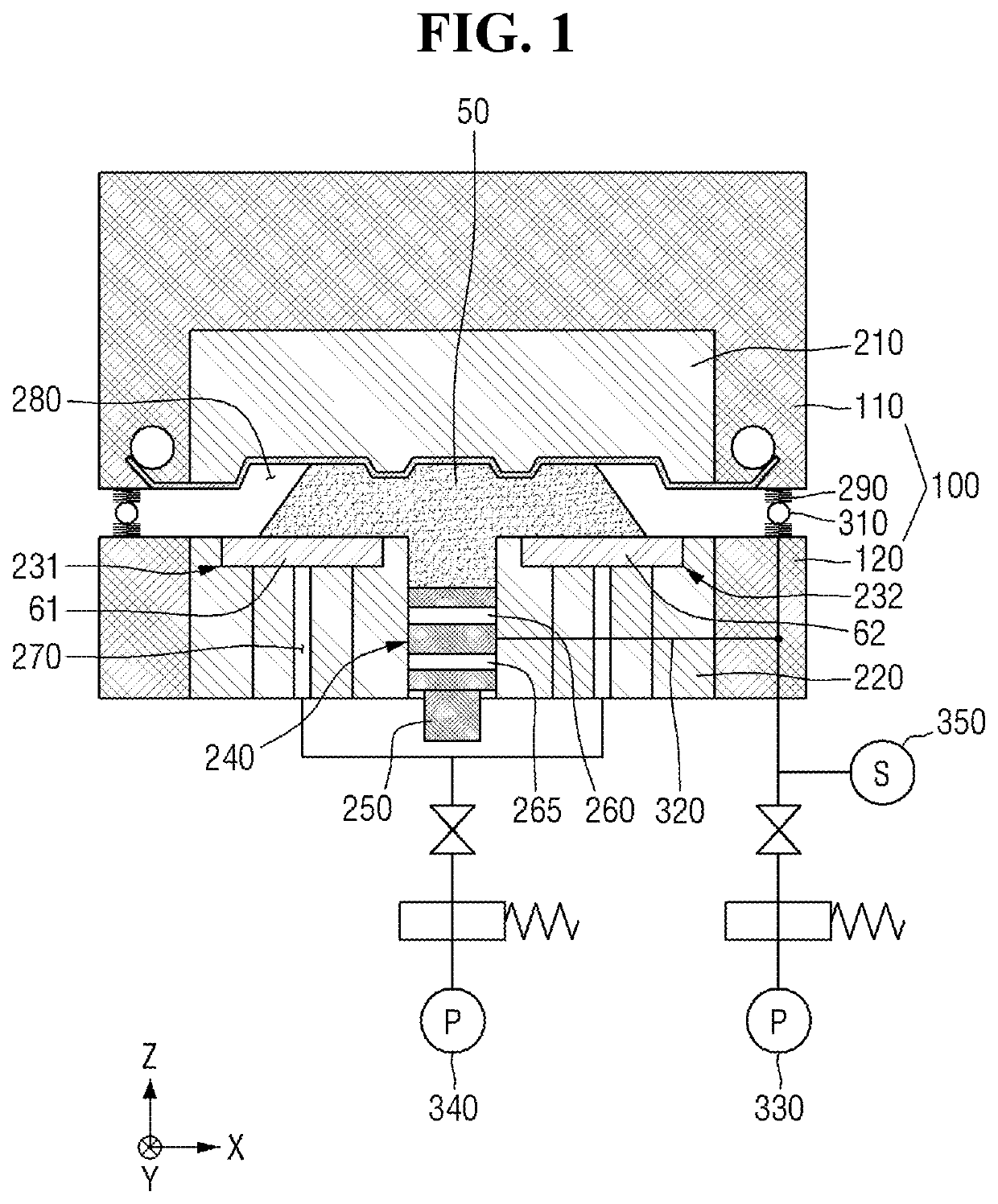
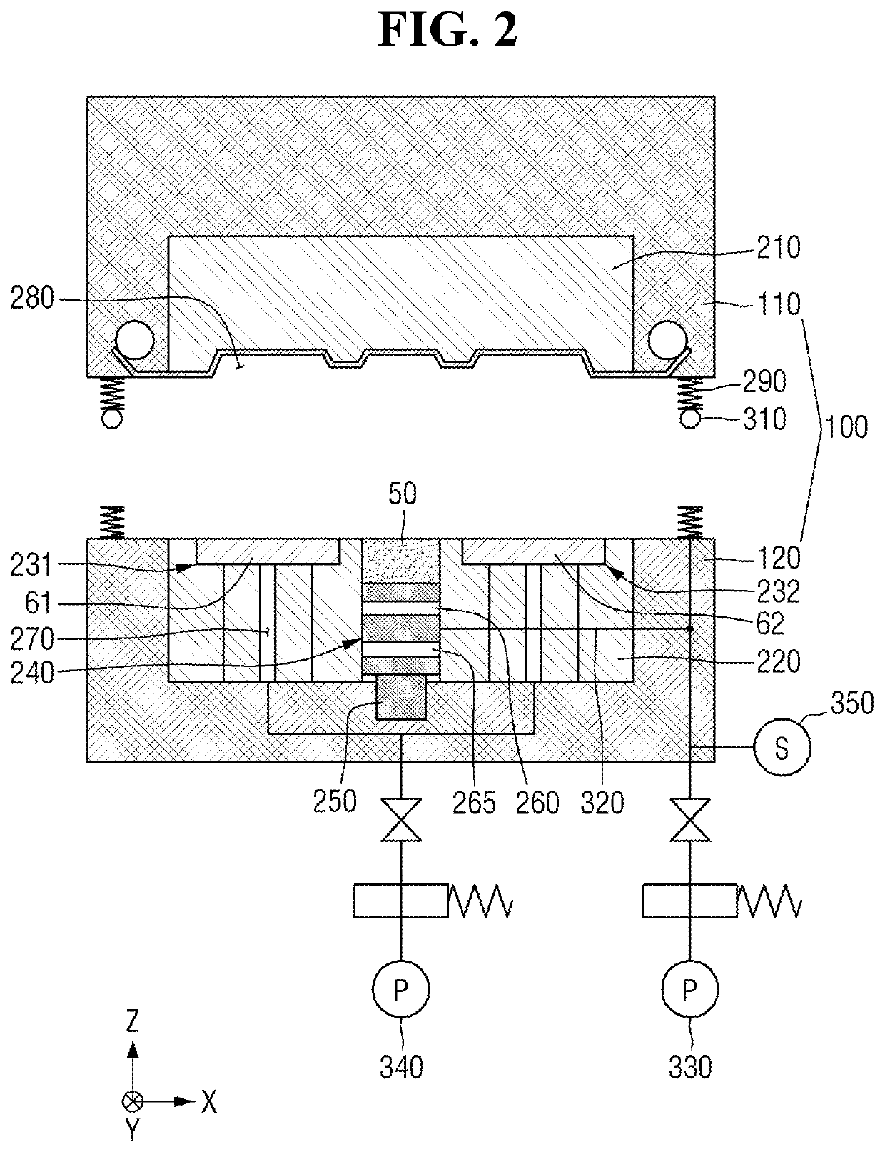
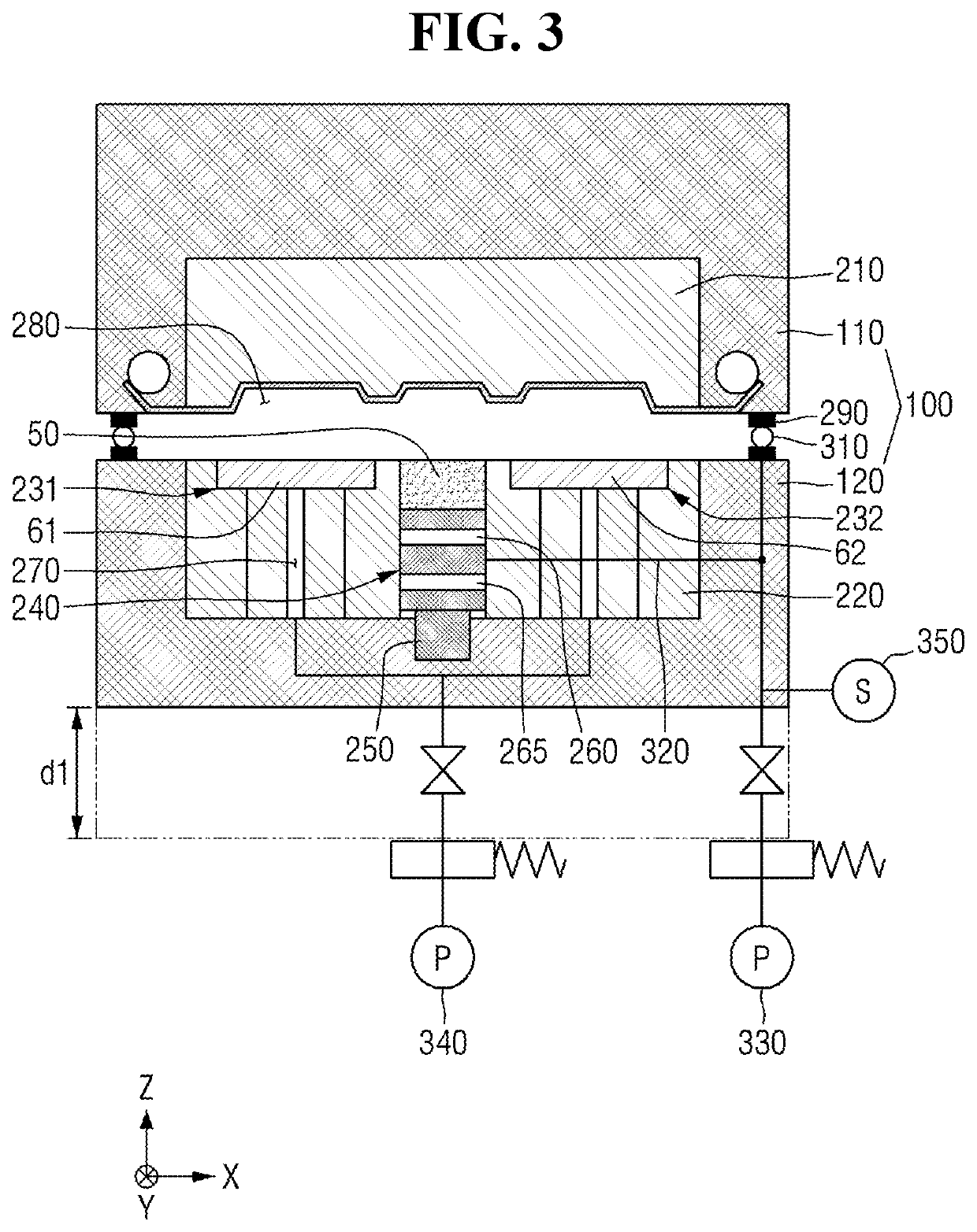
[0026]Hereinafter, a semiconductor device according to some embodiments will be described with reference to FIGS. 1 through 9.
[0027]FIG. 1 is a conceptual diagram of a semiconductor package molding device according to some embodiments.
[0028]Referring to FIG. 1, a first direction X and a second direction Y may be directions intersecting each other among horizontal directions. For example, the first direction X and the second direction Y may be directions perpendicularly intersecting each other. A third direction Z may be a direction intersecting both the first direction X and the second direction Y. For example, the third direction Z may be a direction vertically orthogonal to the first direction X and second direction Y. Accordingly, the first direction X, the second direction Y and the third direction Z may be orthogonal to each other.
[0029]The semiconductor package molding device according to the embodiments includes a chamber 100, an upper mold 210, a lower mold 220, a cavity 280...
PUM
| Property | Measurement | Unit |
|---|---|---|
| sizes | aaaaa | aaaaa |
| sizes | aaaaa | aaaaa |
| sizes | aaaaa | aaaaa |
Abstract
Description
Claims
Application Information
 - R&D
- Intellectual Property
- Life Sciences
- Materials
- Tech Scout
- Unparalleled Data Quality
- Higher Quality Content
- 60% Fewer Hallucinations
Browse by: Latest US Patents, China's latest patents, Technical Efficacy Thesaurus, Application Domain, Technology Topic, Popular Technical Reports.
© 2025 PatSnap. All rights reserved.Legal|Privacy policy|Modern Slavery Act Transparency Statement|Sitemap|About US| Contact US: help@patsnap.com