
Display apparatus

a technology of display apparatus and display panel, which is applied in the direction of instruments, optical elements, optics, etc., can solve the problems of affecting the effect of the display panel

Active Publication Date: 2021-08-10
LG DISPLAY CO LTD
View PDF6 Cites 0 Cited by
  • Summary
  • Abstract
  • Description
  • Claims
  • Application Information

AI Technical Summary

Benefits of technology

The present patent aims to provide a display device that can prevent damage to the organic light emitting layer. By separating the first pattern layer and the second pattern layer, the time exposed to the etching gas during the manufacturing process is reduced, resulting in less damage to the light emitting layer and a lower defect rate for the final display device.

Problems solved by technology

For an organic light emitting display device, in the case that FMM technology is used to form red, green and blue pixels of an organic light emitting layer, it is possible to manufacture a small-to-medium panel by a mask shadow but it is difficult to apply a large area to this panel for a problem of sagging of a deposition mask.
A photographic process has a problem in that the organic light emitting layer is damaged due to an etching gas.
This problem occurs more seriously in a display device, which requires ultra-high resolution, such as a head mounted display (HMD).

Method used


Image

  • Display apparatus
  • Display apparatus
  • Display apparatus

Examples


Embodiment Construction

[0016]Advantages and features of the present disclosure, and implementation methods thereof will be clarified through following aspects described with reference to the accompanying drawings. The present disclosure may, however, be embodied in different forms and should not be construed as limited to the aspects set forth herein. Rather, these aspects are provided so that this disclosure will be thorough and complete, and will fully convey the scope of the present disclosure to those skilled in the art. Further, the present disclosure is only defined by scopes of claims.

[0017]A shape, a size, a ratio, an angle, and a number disclosed in the drawings for describing aspects of the present disclosure are merely an example, and thus, the present disclosure is not limited to the illustrated details. Like reference numerals refer to like elements throughout the specification. In the following description, when the detailed description of the relevant known function or configuration is dete...


PUM

PropertyMeasurementUnit
areaaaaaaaaaaa
defect rateaaaaaaaaaa
sizeaaaaaaaaaa

Abstract

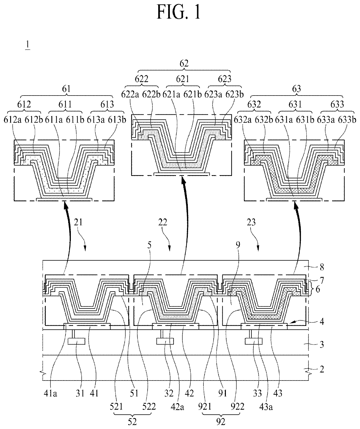
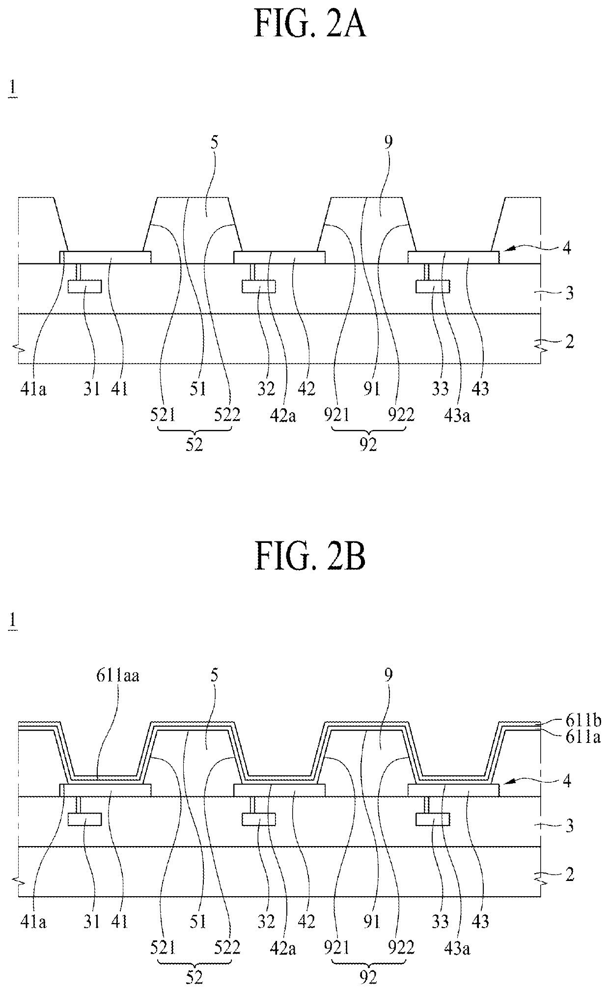
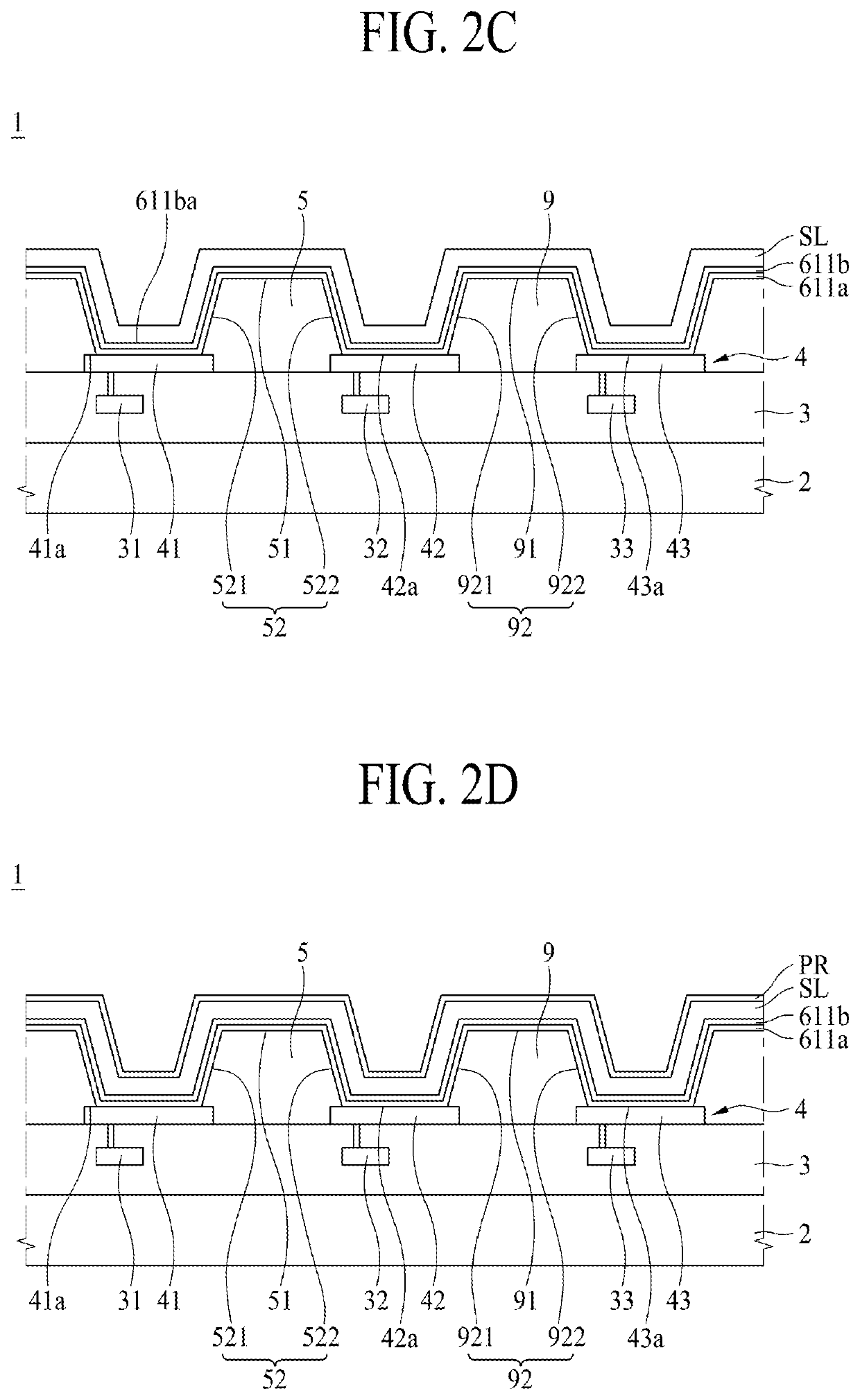
A display device comprises a substrate provided with a first subpixel area and a second subpixel area, a first electrode provided on the substrate, including a first sub electrode provided in the first subpixel area and a second sub electrode provided in the second subpixel area, an organic light emitting layer including a first organic light emitting layer arranged on the first sub electrode and a second organic light emitting layer arranged on the second sub electrode, and a second electrode arranged on the organic light emitting layer, wherein the first organic light emitting layer includes a first pattern layer, a second pattern layer provided on the first pattern layer and a third pattern layer provided on the second pattern layer, the second organic light emitting layer includes a first pattern layer, a second pattern layer provided on the first pattern layer and a third pattern layer provided on the second pattern layer, the first pattern layer of the first organic light emitting layer is spaced apart from the first pattern layer of the second organic light emitting layer, the second pattern layer of the first organic light emitting layer is spaced apart from the second pattern layer of the second organic light emitting layer, and the third pattern layer of the first organic light emitting layer is connected with the third pattern layer of the second organic light emitting layer, and the second pattern layer of the first organic light emitting layer is provided to cover an upper surface and a side of the first pattern layer of the first organic light emitting layer. Therefore, a damage of the light emitting layer can be reduced.

Description

CROSS REFERENCE TO RELATED APPLICATION[0001]This application claims priority from Korean Patent Application No. 10-2018-0142227, filed on Nov. 19, 2018, which is hereby incorporated by reference in its entirety.BACKGROUNDField of the Disclosure[0002]The present disclosure relates to a display device displaying an image.Description of the Background[0003]With the advancement of the information age, the demand for a display device for displaying an image has increased with various forms. Therefore, various types of display devices such as a liquid crystal display (LCD) device, a light emitting display device, an organic light emitting display device, a micro light emitting display device, and a quantum dot light emitting display (QLED) device have been recently used.[0004]For an organic light emitting display device, in the case that FMM technology is used to form red, green and blue pixels of an organic light emitting layer, it is possible to manufacture a small-to-medium panel by a ...

Claims


Application Information

Patent Timeline
Patent Type & Authority Patents(United States)
IPC IPC(8): H01L29/08H01L35/24H01L51/00H01L27/32H01L51/50G02B27/01H10N10/856
CPCH01L27/3206G02B27/0172H01L27/3246H01L51/5036H01L51/5056H01L51/5072H01L51/5088H01L51/5092H01L51/5096G02B2027/0178H10K59/122H10K50/131H10K59/35H10K71/231H10K71/166H10K50/11G02B27/01H10K59/351H10K50/14H10K59/30H10K50/15H10K50/16H10K50/17H10K50/18H10K50/125H10K50/171
Inventor KIM, DAEHEEPARK, JIYOUNGCHOI, HYEJU
Owner LG DISPLAY CO LTD
Learn More