

Pixel array with gate driver and matrix sensor array
a technology of matrix sensor array and gate driver, which is applied in the field of matrix circuit element layout technology, can solve the problems of large amount of pixel units not operating normally, and frameless design cannot be implemented,
- Summary
- Abstract
- Description
- Claims
- Application Information
AI Technical Summary
Benefits of technology
Problems solved by technology
Method used
Image


Examples
first embodiment
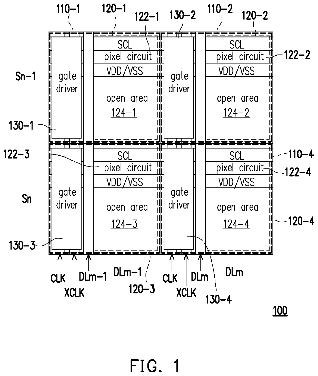
[0031]The quantity of the gate driver 130-1 to 130-4 in each pixel array module 110-1 to 110-4 may be adjusted as required. In the first embodiment, each pixel array module 110-1 to 110-4 has a pixel unit 120-1 to 120-4 and a gate driver 130-1 to 130-4. The gate driver 130-1 to 130-4 in each pixel array module 110-1 to 110-4 is controlled by the gate control signal (e.g., the gate control signal Sn−1 and Sn in FIG. 1) and respectively drives the corresponding pixel unit 120-1 to 120-4 located in the same pixel array module 110-1 to 110-4 according to the time sequence and different column / row directions. In other following embodiments consistent with the disclosure, a pixel array module including one or more pixel units combined with one or more gate drivers will also be exemplified.
[0032]In FIG. 2, the pixel array module 110-1 is taken as an example and the pixel circuit 122-1 and the gate driver 130-1 in the pixel array module 110-1 are illustrated. The gate driver 130-1 includes ...
third embodiment
[0044]Each pixel unit 520-1 to 520-2 in the pixel array module 510-1 respectively includes the pixel circuit 522-1 to 522-2. As such, the single gate driver 130-1 in the third embodiment may drive one or more pixel units (e.g., the pixel units 520-1 to 520-2 shown in FIG. 5A and FIG. 5B) at the same time, thereby improving the open ratio on the overall pixel unit relative to the open area and the light transmittance of the display.
[0045]FIG. 6A is a schematic view of a pixel array 600 with a gate driver according to a fourth embodiment of the disclosure. FIG. 6B is a circuit diagram of a pixel array module 610-1 in FIG. 6A according to the fourth embodiment of the disclosure. Please refer to FIG. 6A and FIG. 6B at the same time. The pixel array 600 according to the fourth embodiment of the disclosure is exemplified using a pixel unit made up of four rows (represented by the gate control signals Sn−1, Sn, Sn+1, and Sn+2) and three columns (represented by the data lines DLm−1, DLm, an...
PUM
| Property | Measurement | Unit |
|---|---|---|
| width | aaaaa | aaaaa |
| aspect ratio | aaaaa | aaaaa |
| width | aaaaa | aaaaa |
Abstract
Description
Claims
Application Information