Touch panel and manufacturing method thereof
a technology of touch panel and manufacturing method, applied in the field of touch panel, can solve problems such as signal interference between them and reduce touch accuracy
- Summary
- Abstract
- Description
- Claims
- Application Information
AI Technical Summary
Benefits of technology
Problems solved by technology
Method used
Image


Examples
Embodiment Construction
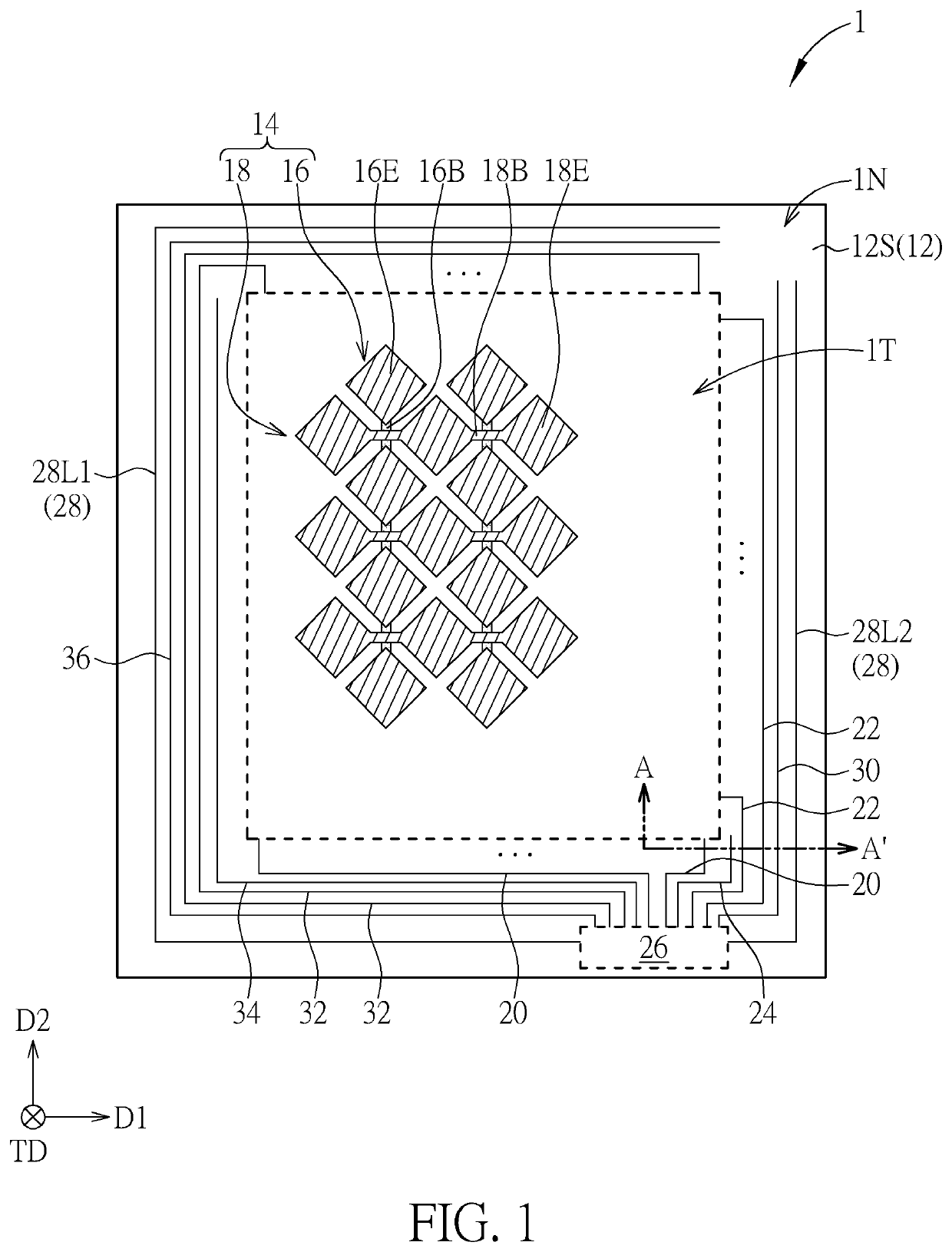
[0015]FIG. 1 schematically illustrates a top view of a touch panel according to a first embodiment of the present invention, and FIG. 2 schematically illustrates a cross-sectional view taken along a line A-A′ of FIG. 1. As shown in FIG. 1 and FIG. 2, the touch panel 1 has a touch region 1T and a trace region 1N disposed at least on one side of the touch region 1T. The touch region 1T may be used for disposing following touch device 14 to detect the position of touch object, and the trace region 1N may be used for disposing following traces, but not limited thereto. In this embodiment, the trace region 1N may surround the touch region 1T, but not limited thereto. In some embodiments, the touch panel 1 may be optionally provided with a light shielding layer (not shown) for shielding the traces in the trace region 1N. When the touch panel 1 is applied to a display device, the touch region 1T may correspond to a display region of the display device for displaying images, and the trace r...
PUM
 Abstract
Description
Claims
Application Information