
Liquid crystal display and manufacturing method thereof

a technology of liquid crystal display and manufacturing method, which is applied in the direction of instruments, semiconductor devices, optics, etc., can solve problems such as display quality degradation, and achieve the effects of reducing the width of the protruding part of the semiconductor pattern, preventing waterfall phenomenon, and improving the display quality of the display devi

Active Publication Date: 2022-01-11
SAMSUNG DISPLAY CO LTD
View PDF9 Cites 0 Cited by
  • Summary
  • Abstract
  • Description
  • Claims
  • Application Information

AI Technical Summary

Benefits of technology

The present patent provides a liquid crystal display that reduces the protruded part of a semiconductor pattern to improve display quality. It also prevents waterfall phenomenon, leakage current, and washed-out color defect. This results in a more stable and high-quality liquid crystal display.

Problems solved by technology

In a process for forming a thin film transistor, a semiconductor layer of the thin film transistor may be etched to have an inclined surface or a protruded portion and it may result in deterioration of a display quality.

Method used


Image

  • Liquid crystal display and manufacturing method thereof
  • Liquid crystal display and manufacturing method thereof
  • Liquid crystal display and manufacturing method thereof

Examples


Embodiment Construction

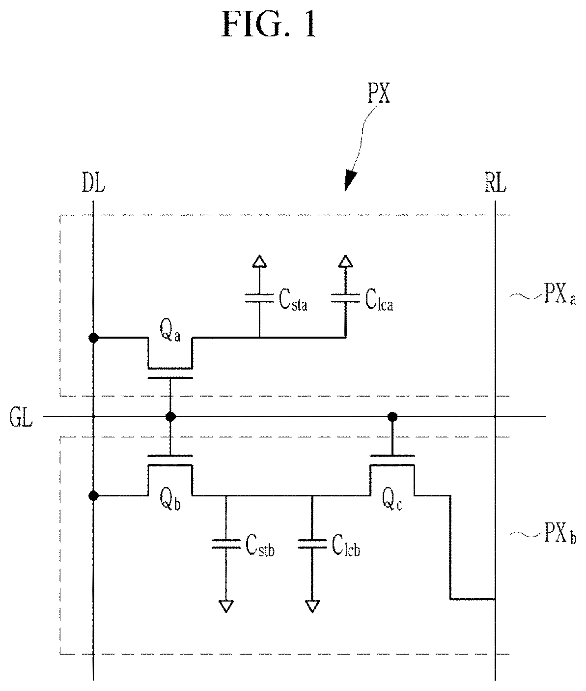
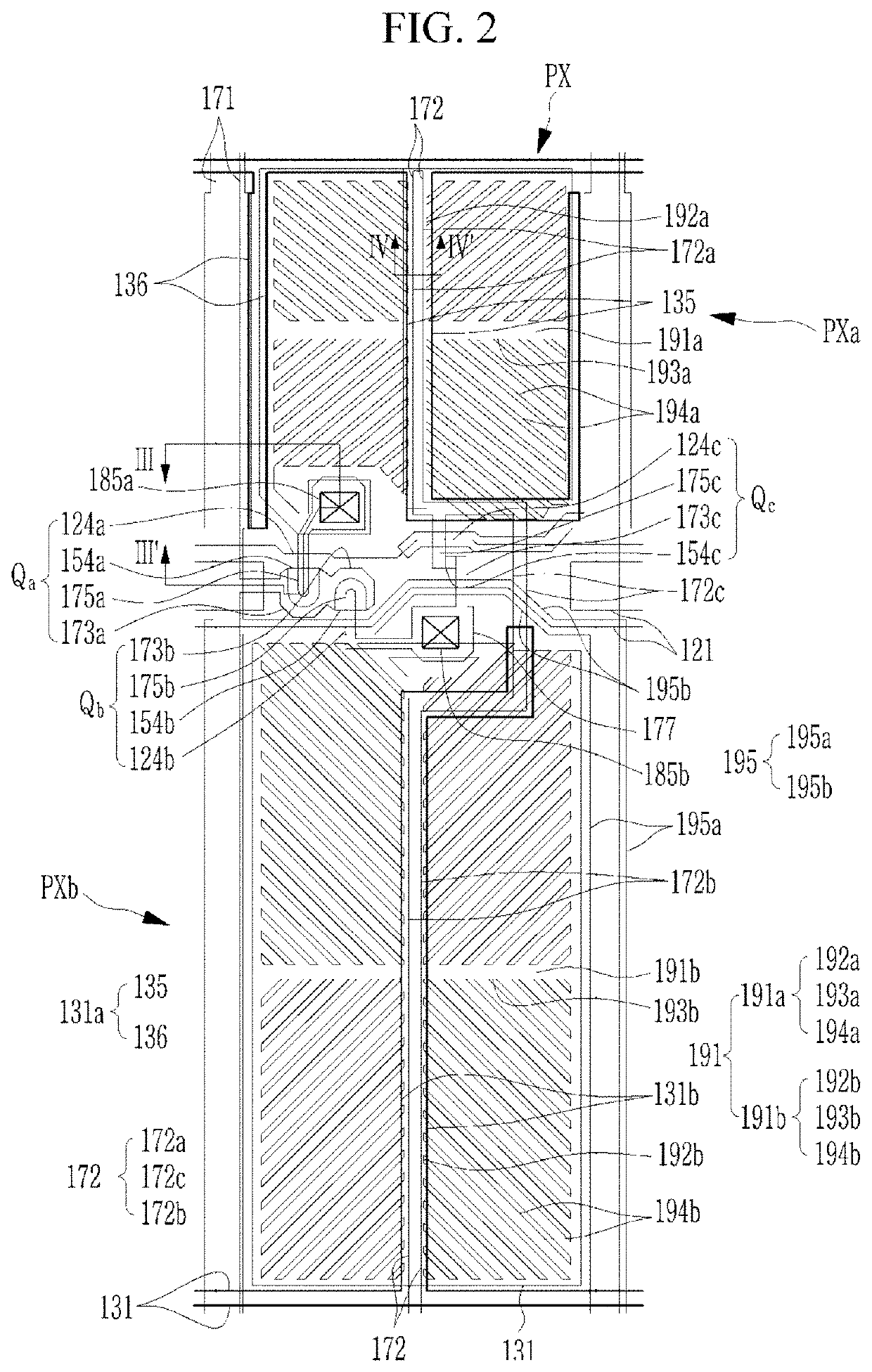
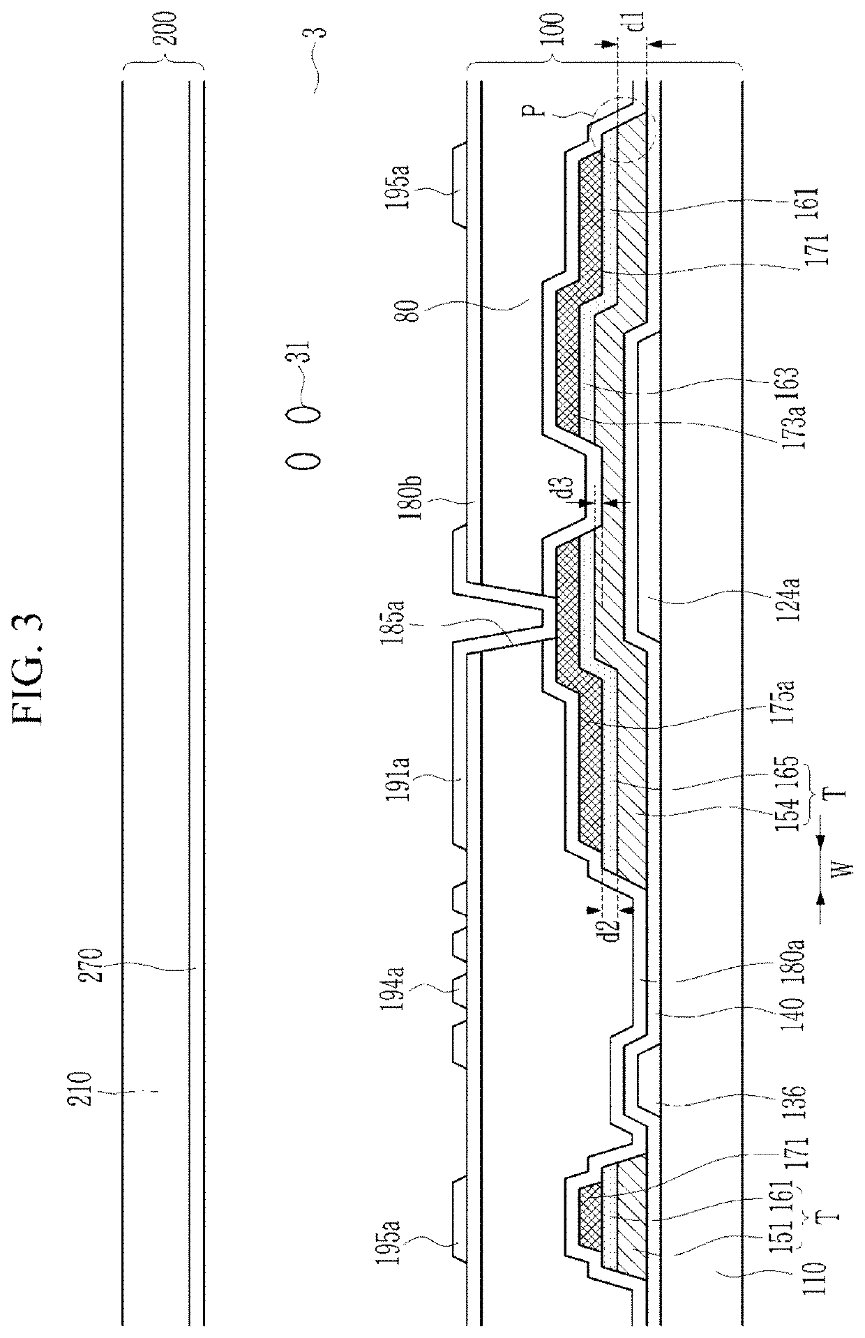
[0038]The present disclosure will be described more fully hereinafter with reference to the accompanying drawings, in which exemplary embodiments of the present disclosure are shown. As those skilled in the art would realize, the described embodiments may be modified in various different ways, without departing from the spirit or scope of the present disclosure.

[0039]In describing the present disclosure, parts that are not related to the description may be omitted. Like reference numerals generally designate like elements throughout the specification.

[0040]In addition, the size and thickness of each configuration shown in the drawings are arbitrarily shown for better understanding and ease of description, but the present disclosure is not limited thereto. In the drawings, the thickness of layers, films, panels, regions, etc., may be exaggerated for clarity. In the drawings, for better understanding and ease of description, the thicknesses of some layers and areas are exaggerated.

[00...


PUM

PropertyMeasurementUnit
color voltage Vssaaaaaaaaaa
widthaaaaaaaaaa
widthaaaaaaaaaa

Abstract

A liquid crystal display includes: a gate line connected to a gate electrode; a semiconductor layer disposed on the gate line and including silicon; an ohmic contact layer disposed on the semiconductor layer; and a data conductor disposed on the ohmic contact layer. The semiconductor layer includes a source region, a drain region, and a channel region disposed between the source region and the drain region. The data conductor includes a data line transmitting a data signal, a source electrode corresponding to the source region, and a drain electrode corresponding to the drain region. A channel step of the semiconductor layer is a height difference between an upper surface in the source region or the drain region and an upper surface in the channel region. The upper surface in the source region or the drain region has a maximum height of the semiconductor layer.

Description

CROSS-REFERENCE TO RELATED APPLICATION[0001]This application claims priority to and the benefit of Korean Patent Application No. 10-2018-0134496 filed in the Korean Intellectual Property Office on Nov. 5, 2018, the disclosure of which is incorporated herein by reference in its entirety.BACKGROUND(a) Technical Field[0002]The present disclosure relates to a liquid crystal display and a manufacturing method thereof.(b) Description of the Related Art[0003]A liquid crystal display (LCD) is the most widely used among various types of flat panel displays. The liquid crystal display includes two display panels that are provided with field generating electrodes such as pixel electrodes and a common electrode, and a liquid crystal layer that is interposed therebetween. The liquid crystal display displays an image using a plurality of pixels. In each pixel, different voltages are applied to the corresponding pixel electrode and the common electrode, and an electric field is generated therebetw...

Claims


Application Information

Patent Timeline
Patent Type & Authority Patents(United States)
IPC IPC(8): G02F1/1368G02F1/1343G02F1/01G02F1/1362G02F1/133
CPCG02F1/1343G02F1/0123G02F1/13306G02F1/136286H01L27/1214H01L27/124H01L27/1259G02F1/1368H01L29/78618H01L29/78696H01L27/1288H01L29/78669H01L29/66765H01L29/78678
Inventor HONG, KI PYONAMGUNG, WANLEEKANG, HYUN SEONGAHN, BYEONG JAE
Owner SAMSUNG DISPLAY CO LTD
Features
  • Generate Ideas
  • Intellectual Property
  • Life Sciences
  • Materials
  • Tech Scout
  • Unparalleled Data Quality
  • Higher Quality Content
  • 60% Fewer Hallucinations
Learn More