Check patentability & draft patents in minutes with Patsnap Eureka AI!

Array substrate, manufacturing method thereof, and display module

a technology of array substrate and manufacturing method, applied in the field of display, can solve the problems of affecting the normal display of the display panel, affecting the electrical properties, etc., and achieve the effect of improving the bending resistance of a thin film transistor and reducing the received bending stress

Active Publication Date: 2022-04-19
WUHAN CHINA STAR OPTOELECTRONICS SEMICON DISPLAY TECH CO LTD
View PDF5 Cites 0 Cited by
  • Summary
  • Abstract
  • Description
  • Claims
  • Application Information

AI Technical Summary

Benefits of technology

The present invention makes a thin film transistor that is more resistant to bending. This is done by adding a second region around the sides of the channel region that is not connected to the source and drain doped regions. This second region helps to reduce the bending stress on the channel region.

Problems solved by technology

This has a negative influence on electrical properties of the thin film transistor device, which in turn affects the normal display of the display panel.

Method used


Image

  • Array substrate, manufacturing method thereof, and display module
  • Array substrate, manufacturing method thereof, and display module
  • Array substrate, manufacturing method thereof, and display module

Examples


Embodiment Construction

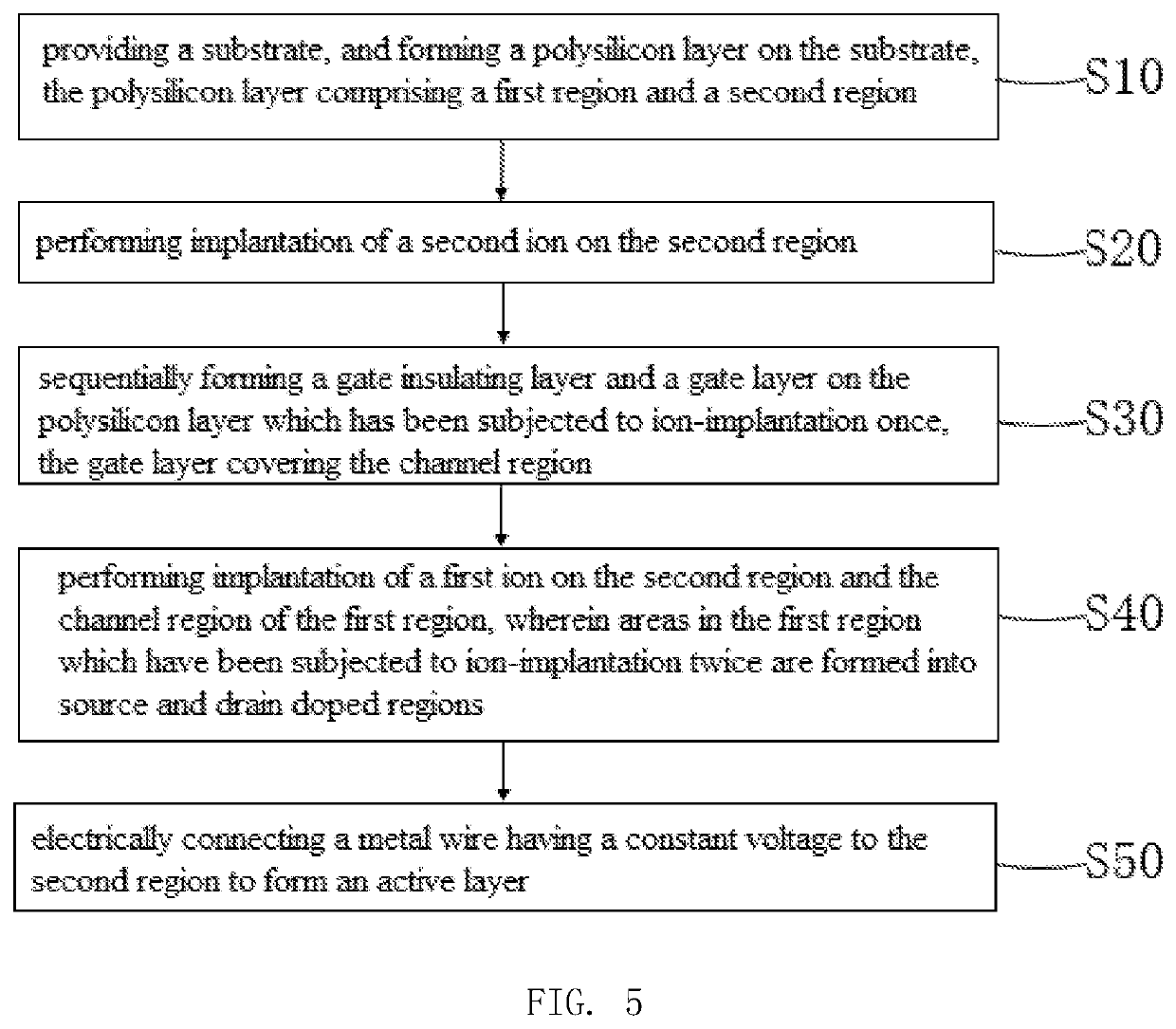
[0040]The following description of the various embodiments is provided to illustrate the specific embodiments of the invention. The spatially relative directional terms mentioned in the present invention, such as “upper”, “lower”, “before”, “after”, “left”, “right”, “inside”, “outside”, “side”, etc. and the like, may be used herein for ease of description to describe one element or feature's relationship to another element(s) or feature(s) as illustrated in the figures which are merely references. The spatially relative terms are intended to encompass different orientations in addition to the orientation as depicted in the figures.

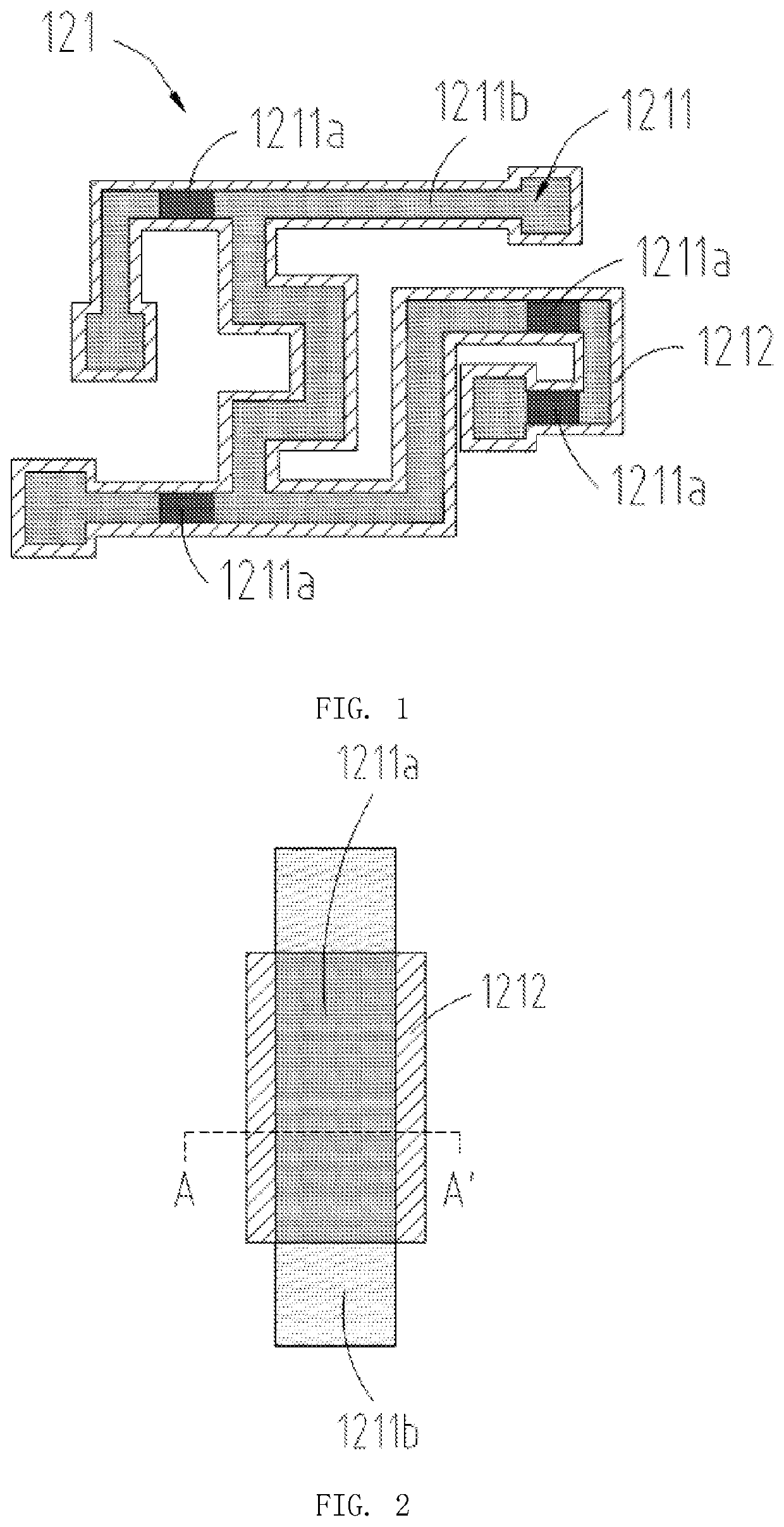
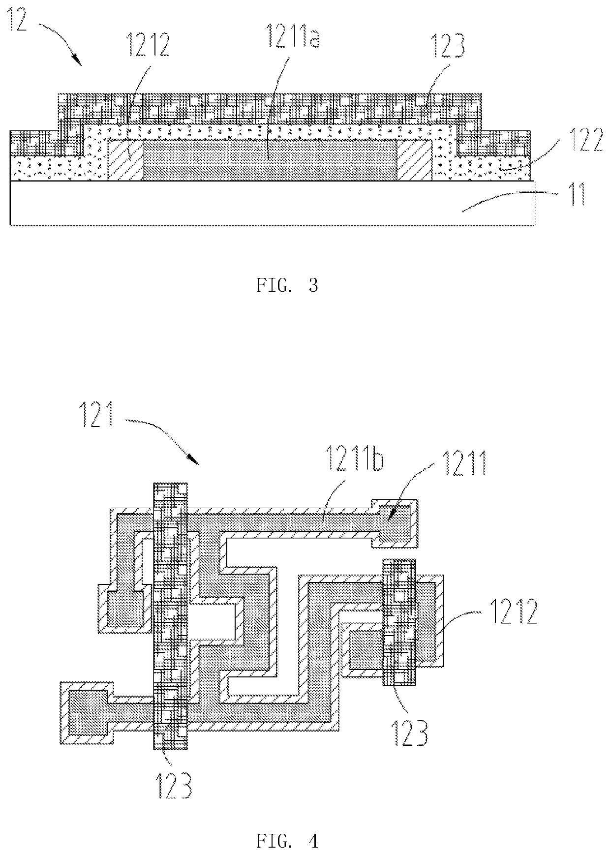
[0041]Referring to FIGS. 1-4, the present invention provides an array substrate including a substrate 11 and a thin film transistor 12 disposed on the substrate 11.

[0042]The substrate 11 is a flexible substrate, and a material for preparing the flexible substrate includes polyimide.

[0043]In an embodiment, a barrier layer and a buffer layer may be further d...


PUM

PropertyMeasurementUnit
thicknessaaaaaaaaaa
constant voltageaaaaaaaaaa
carrier mobilityaaaaaaaaaa

Abstract

The present invention provides an array substrate, a method of fabricating the same, and a display module. The array substrate includes a substrate and a thin film transistor. An active layer of the thin film transistor includes: a first region including source and drain doped regions and a channel region; a second region surrounding at least a side of the channel region not in contact with the source and drain doped regions, and the first region forming a PN junction with the second region.

Description

FIELD OF INVENTION[0001]The present invention relates to the field of display, and in particular, to an array substrate, a manufacturing method thereof, and a display module.DESCRIPTION OF PRIOR ART[0002]Array substrates fabricated using low temperature poly-silicon (LTPS) have high carrier mobility and are therefore the first choice for driving back-plates of flexible display panels. However, in a thin film transistor device structure of the array substrate, a patterned active layer is used as an active layer, and such a structure has its shortcomings that stress concentration occurs at edges of a channel of the active layer under the action of bending stress. This has a negative influence on electrical properties of the thin film transistor device, which in turn affects the normal display of the display panel.[0003]Therefore, there is an urgent need for an array substrate, a method of fabricating the same, and a display module to solve the above problems.SUMMARY OF INVENTION[0004]...

Claims


Application Information

Patent Timeline
Patent Type & Authority Patents(United States)
IPC IPC(8): H01L27/12H01L21/265H01L29/786
CPCH01L27/1222H01L21/26513H01L27/127H01L29/78696
Inventor WANG, WEIHUANG, QING
Owner WUHAN CHINA STAR OPTOELECTRONICS SEMICON DISPLAY TECH CO LTD
Features
  • R&D
  • Intellectual Property
  • Life Sciences
  • Materials
  • Tech Scout
  • Unparalleled Data Quality
  • Higher Quality Content
  • 60% Fewer Hallucinations
Learn More