Semiconductor device
a technology of semiconductor devices and resistors, applied in semiconductor devices, semiconductor/solid-state device details, diodes, etc., can solve the problems of enlargement of semiconductor chips, heat generation, and constant consumption of resistor voltage dividers, so as to increase the resistance of thin film resistors and increase chip size.
- Summary
- Abstract
- Description
- Claims
- Application Information
AI Technical Summary
Benefits of technology
Problems solved by technology
Method used
Image


Examples
embodiment 1
Switching Power Supply Device
[0044]Before describing a semiconductor device 31A according to Embodiment 1 of the present invention, a switching power supply device in which a semiconductor device 31A is used will be described.
[0045]As shown in FIG. 6, a switching power supply device 600A includes the semiconductor device 31A (control IC) of Embodiment 1 of the present invention. The semiconductor device 31A according to Embodiment 1 has: a VH terminal 32 (high breakdown voltage input terminal) to which a voltage of approximately 10V to approximately 500V, for example, is applied; a feedback input terminal 33 (hereinafter referred to as the FB terminal); a current sensing input terminal 34 (hereinafter referred to as the IS terminal); a power supply voltage terminal 35 (hereinafter referred to as the VCC terminal); a gate driving terminal 36 of a MOSFET 19 (hereinafter referred to as the OUT terminal); and a ground terminal 37 (hereinafter referred to as a GND terminal). The VH termi...
modification example of embodiment 1
[0111]Next, a modification example of the semiconductor device 30A of Embodiment 1 will be described with reference to FIGS. 8 and 9.
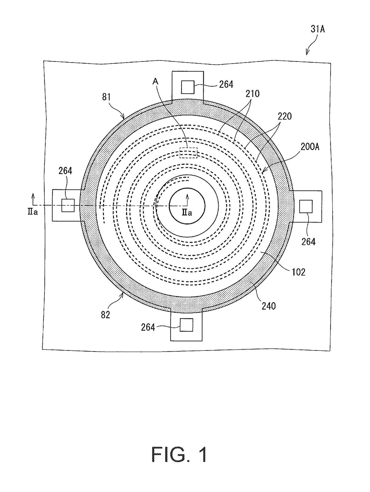
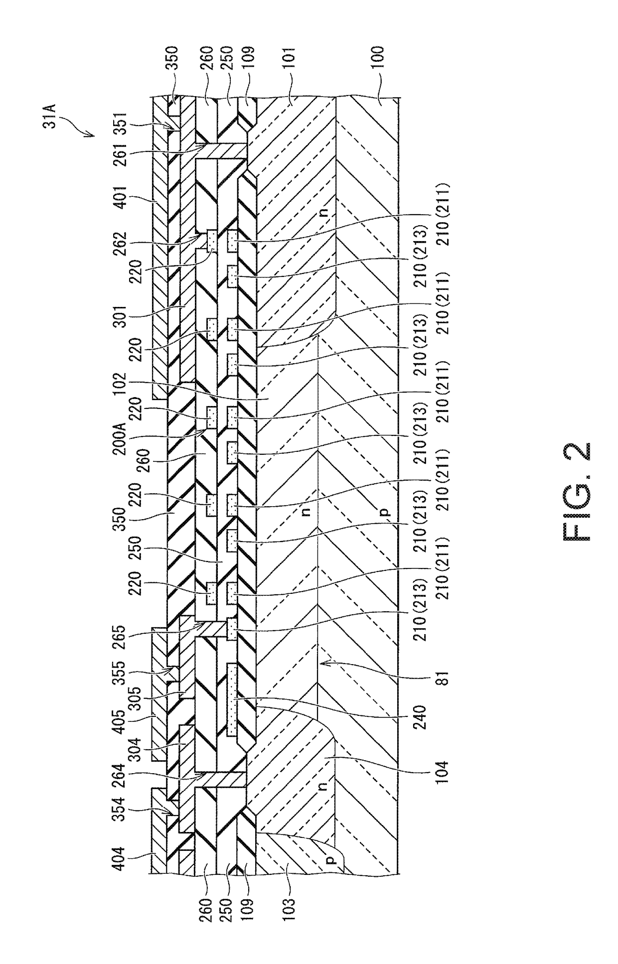
[0112]As shown in FIGS. 3 and 5, a case was described in which the semiconductor device 31A of Embodiment 1 includes the thin film resistor 200A in which the first thin film resistor unit 210 and the second thin film resistor unit 220 are connected to each other through the relay wiring lines 311 and 312. In contrast, as shown in FIGS. 8 and 9, the modification example of the semiconductor device 31A of Embodiment 1 includes a thin film resistor 200A1 in which the first thin film resistor unit 210 and the second thin film resistor unit 220 are connected to each other directly without the use of relay wiring lines. Specifically, the contact section 211a on one end of the first thin film resistor unit 210 is electrically and metallurgically connected directly to the contact section 220a on one end of the second thin film resistor unit 220 through a conta...
embodiment 2
[0116]A semiconductor device 31B according to Embodiment 2 of the present invention has almost the same configuration as the semiconductor device 31A of Embodiment 1, but the configuration of the thin film resistor differs. Below, a thin film resistor 200B of the semiconductor device 31B of Embodiment 2 will be described with reference to FIGS. 10 to 15.
[0117]As shown in FIGS. 10 and 11, the semiconductor device 31B of Embodiment 2 of the present invention includes the thin film resistor 200B. As shown in FIG. 11, the thin film resistor 200B is provided on the drift region 102, which is a voltage withstanding region, of the first and second JFETs 81 and 82 and over the first primary electrode region 101 with the field insulating film 109 therebetween.
[0118]As shown in FIGS. 10 and 12, the thin film resistor 200B has a configuration in which the plurality of first thin film resistor units 230 and the plurality of second thin film resistor units 220 are alternately connected in series...
PUM
 Abstract
Description
Claims
Application Information