Micro-LED chip and manufacturing method thereof, and display panel

a micro-led chip and manufacturing method technology, applied in the field of display technology, can solve the problems of low drive efficiency and increase power consumption, and achieve the effects of improving the high power consumption problem of driving tfts, increasing the voltage, and reducing the power consumption of driving thin film transistors

Active Publication Date: 2022-04-26
SHENZHEN CHINA STAR OPTOELECTRONICS SEMICON DISPLAY TECH CO LTD
View PDF13 Cites 0 Cited by
  • Summary
  • Abstract
  • Description
  • Claims
  • Application Information

AI Technical Summary

Benefits of technology

[0044]The present invention provides a micro-LED chip and a manufacturing method thereof, wherein the micro-LED chip comprises a buffer layer, a first semiconductor layer, an active layer, a second semiconductor layer, an insulating layer, a current diffusion layer, a protective layer, and a first electrode and a second electrode which are stacked on each other. The insulating layer divides the first semiconductor layer, the active layer, and the second semiconductor layer into at least two sub-chips separated from each other, the second semiconductor layer in each sub-chip is connected to the first semiconductor layer in the next sub-chip via the current diffusion layer, the first electrode is electrically connected to the first semiconductor layer of the first sub-chip, and the second electrode is electrically connected to the second semiconductor layer of the last sub-chip. The sub-chips are separated by the insulating layer, and the sub-chips are connected in series by the current diffusion layer, thereby increasing a voltage across the micro-LED, reducing power consumption of a driving thin film transistor (TFT), and improving a high power consumption problem of driving TFTs of conventional micro-LED displays.

Problems solved by technology

However, since a driving thin film transistor (TFT) mainly works in a saturation region during display, a voltage across a source electrode and a drain electrode of the TFT is large, but the voltage across the micro-LED is low, which increases power consumption and leads to low drive efficiency.

Method used


Image

  • Micro-LED chip and manufacturing method thereof, and display panel
  • Micro-LED chip and manufacturing method thereof, and display panel
  • Micro-LED chip and manufacturing method thereof, and display panel

Examples


Embodiment Construction

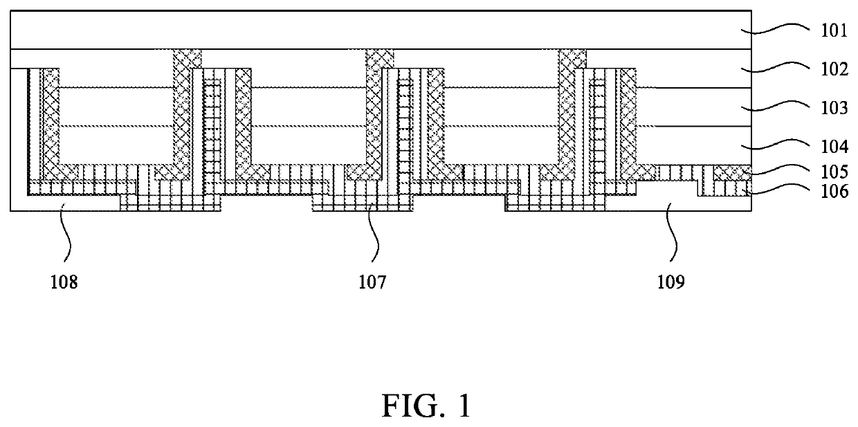
[0049]Embodiments of the present invention are described in detail below with reference to the accompanying drawings. The directional terms in the present disclosure, such as “upper”, “lower”, “front”, “rear”, “left”, “right”, “inside”, “outside”, and “lateral”, are merely illustrative with reference to the accompanying drawings, and are not intended to limit the protection scope of the present application. In the drawings, the same reference numerals in the drawings denote the same elements.

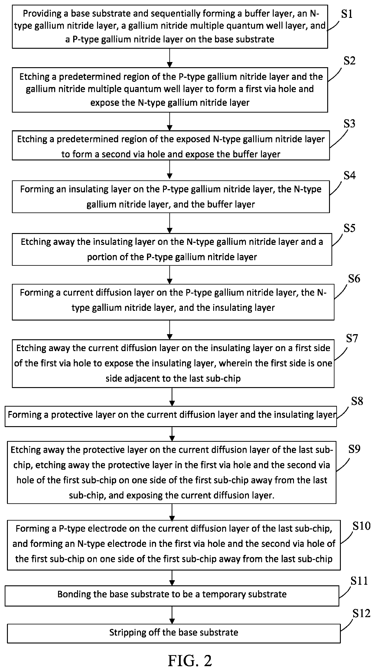
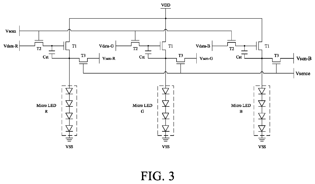
[0050]In view of a high power consumption problem of driving thin film transistors (TFTs) in conventional micro-LED displays, the present invention provides a micro-LED chip to solve this problem.

[0051]In one embodiment, as shown FIG. 1, the present application provides a micro LED chip comprises the following sequentially stacked on each other from top to bottom:

[0052]A buffer layer 101: In an embodiment, the buffer layer 101 is an intrinsic gallium nitride layer with a thick thickness greater ...


PUM

PropertyMeasurementUnit
thicknessaaaaaaaaaa
current diffusionaaaaaaaaaa
semiconductoraaaaaaaaaa

Abstract

The present invention provides a micro-LED chip, a manufacturing method of the micro-LED chip, and a display panel. The micro-LED chip includes a plurality of sub-chips connected in series. The first sub-chip and the last sub-chip are connected to a first electrode and a second electrode, respectively. Accordingly, a voltage across the micro-LED chip is increased, power consumption of a driving thin film transistor (TFT) is reduced, and a high power consumption problem of driving TFTs in conventional micro-LED displays is improved.

Description

[0001]This application claims priority to Chinese patent application no. 201910466611.8, entitled “Micro-LED Chip and Manufacturing Method thereof, and Display Panel”, filed on May 31, 2019, and the entire contents of which are incorporated by reference in this application.1. FIELD OF DISCLOSURE[0002]The present invention relates to a field of display technology and in particular, to a micro-LED chip and a manufacturing method thereof, and a display panel.2. DESCRIPTION OF RELATED ART[0003]Micro-LEDs have become the focus of next-generation display technology due to their higher brightness, better luminous efficiency, and lower power consumption.[0004]However, since a driving thin film transistor (TFT) mainly works in a saturation region during display, a voltage across a source electrode and a drain electrode of the TFT is large, but the voltage across the micro-LED is low, which increases power consumption and leads to low drive efficiency.[0005]Therefore, there is a need to provi...

Claims


Application Information

Patent Timeline
Patent Type & Authority Patents(United States)
IPC IPC(8): H01L33/08H01L33/00H01L33/38H01L33/40H01L25/16H01L33/06H01L33/32
CPCH01L33/08H01L25/167H01L33/007H01L33/0093H01L33/382H01L33/405H01L33/06H01L33/32H01L2933/0016H01L33/44H01L33/14H01L27/156H01L33/38H01L25/0753H01L2933/0066H01L33/62
Inventor FAN, YONG
Owner SHENZHEN CHINA STAR OPTOELECTRONICS SEMICON DISPLAY TECH CO LTD
Why Eureka
Try Eureka