Supercharge Your Innovation With Domain-Expert AI Agents!

Wiring board manufacturing method

a manufacturing method and wire technology, applied in the manufacture of multilayer circuits, printed circuits, printed circuit simultaneous processing, etc., can solve the problems of blade slippage, wiring layer damage, and possible damage to a wiring layer

Active Publication Date: 2022-04-26
MITSUI MINING & SMELTING CO LTD
View PDF13 Cites 0 Cited by
  • Summary
  • Abstract
  • Description
  • Claims
  • Application Information

AI Technical Summary

Benefits of technology

The present patent is about a new process for making a composite laminate that prevents defects, such as breaking in the support and cracking and wire disconnections in the multilayered circuit board, and ensures stable release of the support or the multilayered circuit board during manufacturing of a circuit board. The technical effect of this process is to improve the quality and reliability of the circuit board manufacturing process.

Problems solved by technology

Unfortunately, the technique using the blades in Patent Literature 1 is likely to damage a wiring layer.
For example, the blades may slip to damage the wiring layer.
In some cases, the wiring layer may be damaged by local stress in the interface adjacent to the release layer during insertion or movement of the blades.

Method used


Image

  • Wiring board manufacturing method
  • Wiring board manufacturing method
  • Wiring board manufacturing method

Examples


examples

[0066]The present invention will be described in more detail with reference to the following Examples.

examples 1 to 5

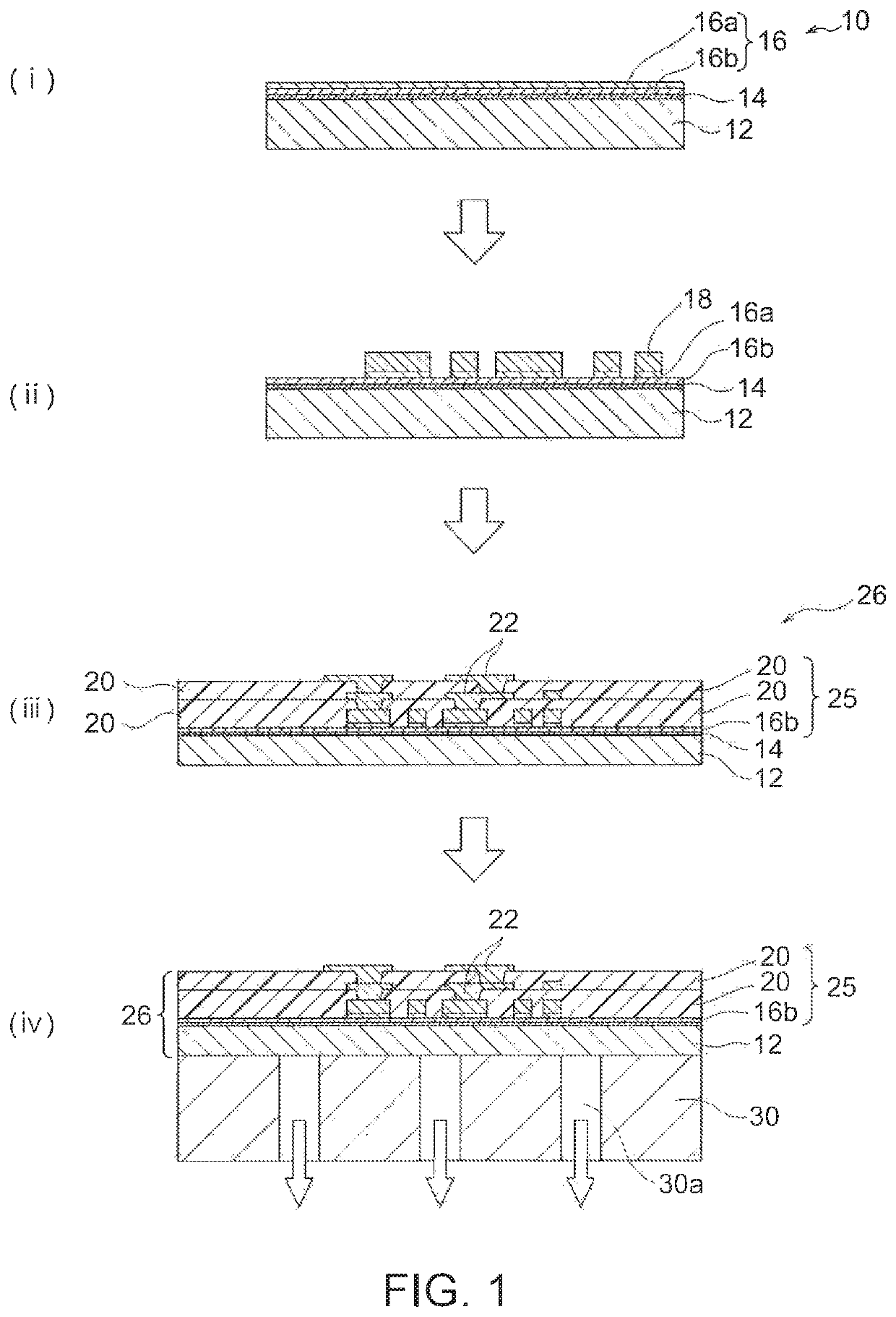
[0067](1) Production of Multilayered Laminate

[0068]A soda glass plate having a thickness of 1.1 mm was prepared as a support or carrier. An adhesive metal layer (a titanium layer having a thickness of 100 nm), an auxiliary release layer (a copper layer having a thickness of 100 nm), a release layer (an amorphous carbon layer having a thickness of 3 nm), and an extremely thin copper layer (a copper layer having a thickness of 300 nm) were in sequence formed on the soda glass plate through a sputtering process, resulting in a cupper foil with a carrier. A multilayered circuit board including a wiring layer having a two-layer structure (a composite layer consisting of an insulating layer and a wiring layer and having a total thickness of 0.03 mm. The wiring layer on the release layer had a width of 10 μm) was formed on the extremely thin copper layer of the resultant cupper foil with a carrier through a build-up process, resulting in a composite laminate having dimensions of 510 mm by ...


PUM


Abstract

Provided is a method of manufacturing a circuit board involves: preparing a composite laminate including a support, a release layer, and a multilayered circuit board; disposing the composite laminate on a stage such that one face of the composite laminate is put into tight contact with the stage; and releasing the support or the multilayered circuit board from the release layer such that the support or the multilayered circuit board forms a convex face with a curvature radius of 200 to 5000 mm while the face of the composite laminate is kept in tight contact with the stage. The method according to the present invention can prevent the occurrences of defects, for example, breaking in the support and cracking and wire disconnections in the multilayered circuit board in manufacturing of circuit boards, such as coreless circuit boards, and ensure stable release of the support or the multilayered circuit board.

Description

TECHNICAL FILED[0001]The present invention relates to a method of manufacturing a circuit board.BACKGROUND ART[0002]In manufacturing of coreless circuit boards through, for example, a coreless build-up process, a composite laminate including a support, a release layer, and a multilayered circuit board is prepared, and the support is released from the composite laminate to leave the multilayered circuit board. In traditional common techniques, the support or the multilayered circuit board is gripped at its end for a mechanical release of the support.[0003]In the latest trends, rigid supports increase whereas thicknesses of multilayered circuit boards decrease. Unfortunately, the release of supports in such a circumstance causes breaking of the supports and cracking and wire disconnections in the multilayered circuit boards.[0004]Various methods of releasing the supports in manufacturing of coreless circuit boards have been proposed. For example, Patent Literature 1 (JP2015-005644A) d...

Claims


Application Information

Patent Timeline
Patent Type & Authority Patents(United States)
IPC IPC(8): H05K3/46H05K3/00
CPCH05K3/4682H05K3/0097H05K3/4652H05K2203/0143H05K2203/1536H05K2203/082
Inventor NAKAMURA, TOSHIMIMATSUURA, YOSHINORI
Owner MITSUI MINING & SMELTING CO LTD
Features
  • R&D
  • Intellectual Property
  • Life Sciences
  • Materials
  • Tech Scout
  • Unparalleled Data Quality
  • Higher Quality Content
  • 60% Fewer Hallucinations
Learn More