
Micro light emitting element and image display device

a light emitting element and image technology, applied in the direction of basic electric elements, semiconductor devices, electrical equipment, etc., can solve the problems of large amount of light loss, decrease in color purity, and decrease in contras

Active Publication Date: 2022-07-26
SHARP FUKUYAMA LASER CO LTD
View PDF7 Cites 2 Cited by
  • Summary
  • Abstract
  • Description
  • Claims
  • Application Information

AI Technical Summary

Benefits of technology

This configuration prevents optical crosstalk and improves light extraction efficiency, leading to enhanced light emission efficiency and reduced power consumption.

Problems solved by technology

However, there are the following problems in structures of the micro light emitting element and the display element disclosed in the above-mentioned Japanese Patent Application Publication No. 2002-141492.
Such optical crosstalk causes problems such as a decrease in contrast and a decrease in color purity.
In the technique disclosed in Japanese Patent Application Publication No. 2002-141492, a large amount of light is lost due to the light emission from the side surface of the micro light emitting element, and the light generated in the light emission layer of the micro light emitting element is trapped inside the micro light emitting element.
Due to the causes, the light extraction efficiency of the micro light emitting element becomes low and thus the light emission efficiency becomes low.
The decrease in light emission efficiency causes problems such as an increase in power consumption and an increase in temperature due to heat generation.

Method used


Image

  • Micro light emitting element and image display device
  • Micro light emitting element and image display device
  • Micro light emitting element and image display device

Examples


first embodiment

Configuration of Image Display Device 200

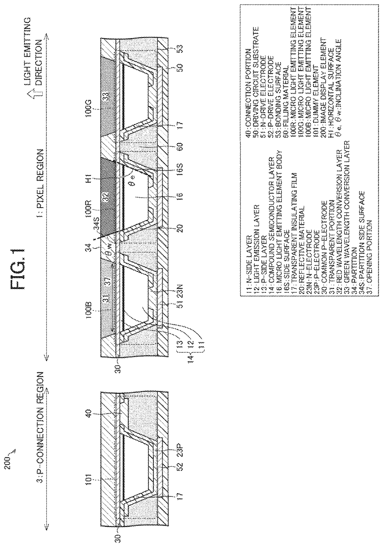
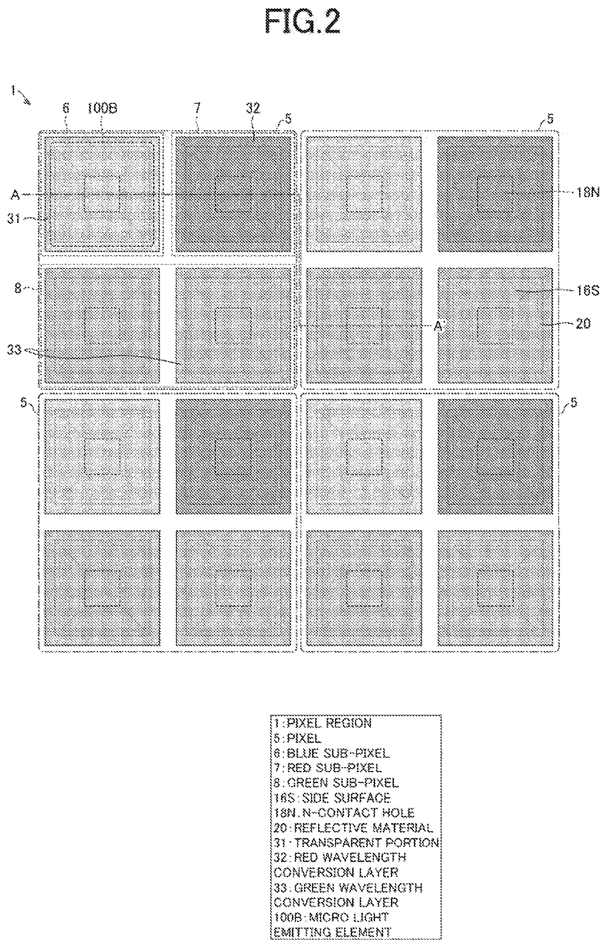
[0040]FIG. 1 is a schematic cross-sectional view of an image display device 200 according to a first embodiment of the present disclosure. FIG. 2 is a schematic plan view of a pixel region of the image display device 200 according to the first embodiment of the present disclosure. Hereinafter, the image display device 200 will be described with the image display device 200 having a plurality of micro light emitting elements 100 as an example with reference to FIGS. 1 to 8.

[0041]In the description of a configuration of the image display device 200, a light emitting surface is referred to as an upper surface, a surface opposite to the light emitting surface side is referred to as a lower surface, and a surface on a side other than the upper surface and the lower surface is referred to as a side surface. In the micro light emitting element 100, up and down directions are indicated by having a light emitting surface side as an upper side and havi...

second embodiment

Configuration of Image Display Device 200a

[0139]A second embodiment of the present disclosure will be described below with reference to FIGS. 13 to 19. For convenience of description, members having the same functions as those described in the first embodiment will be designated by the same reference numerals, and the description thereof will not be repeated. An image display device 200a according to the second embodiment is different from the image display device 200 according to the first embodiment in the shape of a body 16a of a micro light emitting element 100a, the configuration of a partition 34a, and the configuration of the common P-electrode 30a.

[0140]In the present embodiment, as shown in FIG. 13, a side surface 16Sa of the body 16a of the micro light emitting element 100a has a first side surface 16Sa1 and a second side surface 16Sa2. The first side surface 16Sa1 is located on a bottom portion side of the side surface 16Sa and forms a first inclination angle θe1 by the...

third embodiment

Configuration of Image Display Device 200b

[0157]A third embodiment of the present disclosure will be described below with reference to FIG. 20. For convenience of description, members having the same functions as the members described in the above embodiments are designated by the same reference numerals, and the description thereof will not be repeated. An image display device 200b according to the third embodiment has a configuration similar to that of the second embodiment, but the shape of a body 16b is different.

[0158]In the second embodiment, the inclination angle is θe12, and the first side surface 16Sa1 inclined at the small first inclination angle θe1 is disposed on the side opposite to the light emitting surface side with respect to the second side surface 16Sa2 inclined at the large second inclination angle θe2. On the contrary, in the present embodiment, a first side surface 16Sb11 inclined at a small first inclination angle θe11 is disposed on the light emitting surfac...


PUM

PropertyMeasurementUnit
inclination angleaaaaaaaaaa
thicknessaaaaaaaaaa
thicknessaaaaaaaaaa

Abstract

A micro light emitting element includes: a body including a compound semiconductor layer in which a first conductive layer, a light emission layer, and a second conductive layer with a conductive type opposite to a conductive type of the first conductive layer are stacked in order from a light emitting surface side; a first electrode including a transparent electrode on the light emitting surface side; a second electrode including a metal film on a side opposite to the light emitting surface side; and a first reflective material covering a side surface of the body. The light emission layer is disposed on the light emitting surface side of the body. The side surface of the body is tapered at an inclination angle to open in a light emitting direction.

Description

CROSS REFERENCE TO RELATED APPLICATION[0001]The present application claims priority from Japanese Patent Application No. 2019-132062, filed Jul. 17, 2019, the entire contents of which are hereby incorporated by reference into this application.BACKGROUND OF THE INVENTION1. Field of the Invention[0002]The present disclosure relates to a micro light emitting element and an image display device including a micro light emitting element.2. Description of the Related Art[0003]In the related art, there is proposed a display element in which a plurality of micro light emitting elements constituting pixels are disposed on a driving circuit substrate. For example, in a technique disclosed in Japanese Patent Application Publication No. 2002-141492, a driving circuit is formed on a silicon substrate and a minute light emitting diode (LED) array that emits ultraviolet light is disposed on the driving circuit. The above technique discloses a small display element in which a wavelength conversion l...

Claims


Application Information

Patent Timeline
Patent Type & Authority Patents(United States)
IPC IPC(8): H01L33/20H01L33/40H01L33/38H01L33/60H01L33/44H01L33/50H01L33/32H01L25/16H01L33/00
CPCH01L25/167H01L33/20H01L33/385H01L33/405H01L33/60H01L33/0093H01L33/32H01L33/44H01L33/505H01L2933/0016H01L2933/0025H01L33/42H01L33/50H01L27/156H01L33/46H01L25/0753H01L33/504
Inventor IGUCHI, KATSUJIKAWANISHI, HIDENORI
Owner SHARP FUKUYAMA LASER CO LTD
Learn More