Electronic device and antenna structure thereof

a technology of electronic devices and antennas, applied in the direction of polarised antenna unit combinations, resonant antennas, antenna earthings, etc., can solve the problems of relatively difficult design of broadband antenna structures encompassing both the n257 band and the n260 band, and achieve the effect of improving the impedance bandwidth of the antenna structure having a single feed, improving the impedance matching between the first operating frequency band and the second operating frequency band, and increasing the bandwidth of the low frequency

Active Publication Date: 2022-10-11
PEGATRON
View PDF12 Cites 0 Cited by
  • Summary
  • Abstract
  • Description
  • Claims
  • Application Information

AI Technical Summary

Benefits of technology

[0009]One of the beneficial effects of the electronic device and the antenna structure thereof of the present disclosure is that, impedance matching between a first operating frequency band and a second operating frequency band is improved by virtue of “the feeding member” and “a first predetermined gap between the feeding member and the first radiating member”. In addition, the bandwidth of the low frequency band is increased by virtue of “a second predetermined gap defined between the main body and the first radiating member” and “a path that electrically connects the second radiating member with the grounding member”, such that an impedance bandwidth of the antenna structure having a single feed is increased and that the impedance matching is enhanced.

Problems solved by technology

However, since the frequency of the n257 band is close to that of the n260 band, designing a broadband antenna structure encompassing both the n257 band and the n260 band is relatively difficult.

Method used


Image

  • Electronic device and antenna structure thereof
  • Electronic device and antenna structure thereof
  • Electronic device and antenna structure thereof

Examples


first embodiment

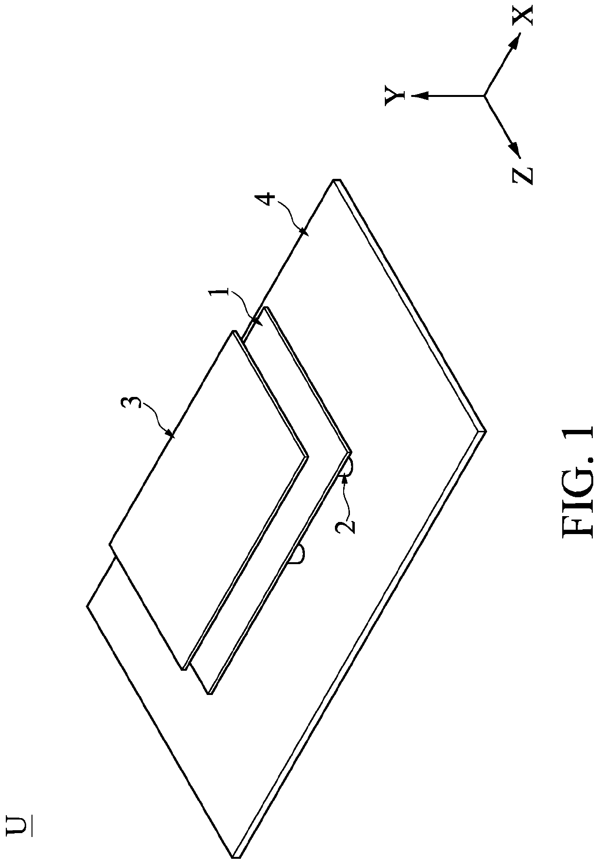
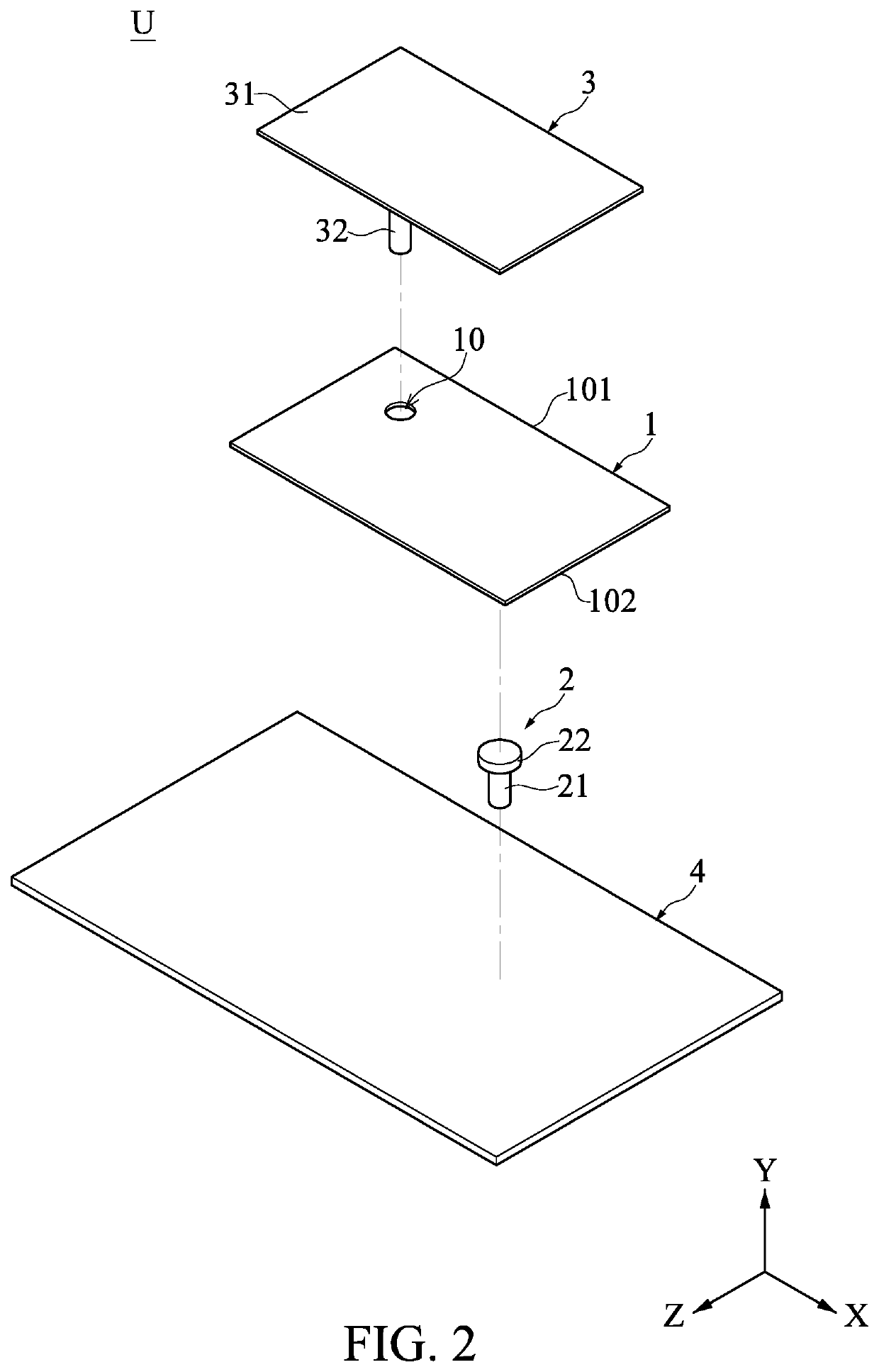
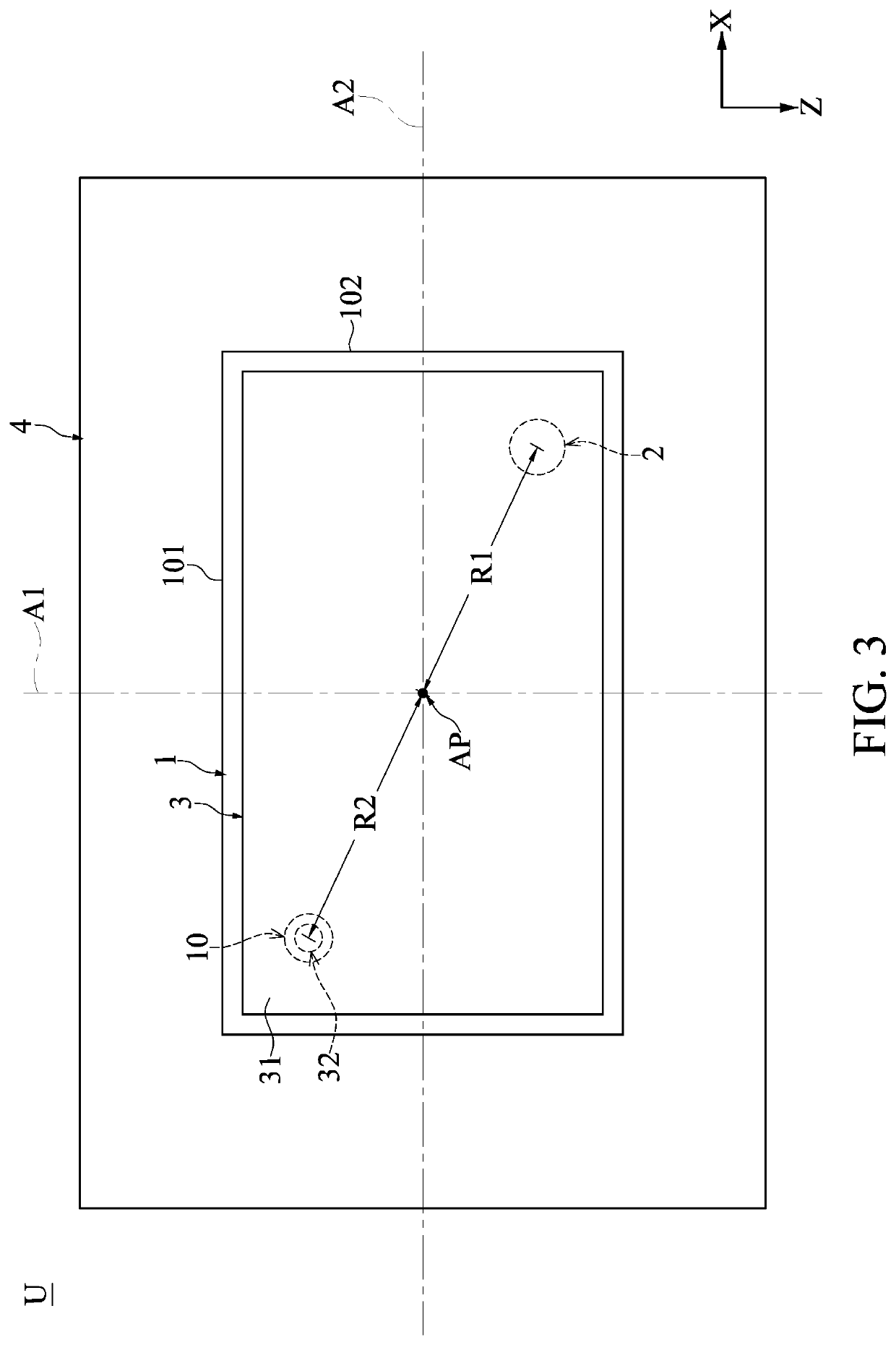
[0027]References are made to FIG. 1 to FIG. 4, which are perspective schematic views of an antenna structure in a first embodiment of the present disclosure. An antenna structure U is provided by the present disclosure, and an overall structure of the antenna structure U is illustrated in the first embodiment. An electronic device D utilizing the antenna structure U is also provided by the present disclosure, and a structure of the electronic device D is illustrated in the following embodiment.

[0028]The antenna structure U includes a first radiating member 1, a feeding member 2, a second radiating member 3, and a grounding member 4. For example, the antenna structure U of the present disclosure may be a patch antenna, and the second radiating member 3, the first radiating member 1, the feeding member 2, and the grounding member 4 may be respective metal layers that are disposed on a multi-layer board structure and stacked sequentially upon one another, but the present disclosure is ...

second embodiment

[0043]Firstly, references are made to FIG. 13 and FIG. 14, which are functional block diagrams of an electronic device in a second embodiment of the present disclosure. The second embodiment of the present disclosure provides an electronic device D including a plurality of antenna arrays UG, a plurality of signal sources S, and a radio frequency (RF) chip F. In the present disclosure, the electronic device D includes at least two adjacent antenna structures U in different polarization directions, and the two adjacent antenna structures U in different polarization directions may form one of the antenna arrays UG in the electronic device D. That is, each of the antenna arrays UG includes two adjacent antenna structures U in different polarization directions. The implementation shown in FIG. 13 is a 1×4 antenna array, and the implementation shown in FIG. 14 is a 2×2 antenna array. However, it should be noted that in other implementations, antenna arrays in any other forms may also be u...


PUM


Abstract

An electronic device and an antenna structure thereof are provided. The antenna structure includes a first radiating member, a feeding member disposed on the first radiating member, a second radiating member, and a grounding member. A first predetermined gap is between the feeding member and the first radiating member. The feeding member, the first predetermined gap, and the first radiating member resonate to generate a low frequency band and a high frequency band. The second radiating member including a main body and a grounding part is disposed on the first radiating member. A second predetermined gap is between the main body and the first radiating member. The grounding part, the main body, and the second predetermined gap resonate to increase a bandwidth of the low frequency band. The grounding member is disposed on the first radiating member and electrically connected to the grounding part.

Description

CROSS-REFERENCE TO RELATED PATENT APPLICATION[0001]This application claims the benefit of priority to Taiwan Patent Application No. 108147531, filed on Dec. 25, 2019. The entire content of the above identified application is incorporated herein by reference.[0002]Some references, which may include patents, patent applications and various publications, may be cited and discussed in the description of this disclosure. The citation and / or discussion of such references is provided merely to clarify the description of the present disclosure and is not an admission that any such reference is “prior art” to the disclosure described herein. All references cited and discussed in this specification are incorporated herein by reference in their entireties and to the same extent as if each reference was individually incorporated by reference.TECHNOLOGY FIELD[0003]The present disclosure relates to an antenna structure, and more particularly to an electronic device and an antenna structure thereo...

Claims


Application Information

Patent Timeline
Patent Type & Authority Patents(United States)
IPC IPC(8): H01Q1/50H01Q5/335H01Q1/48H01Q9/04H04B1/18
CPCH01Q5/335H01Q1/48H01Q9/0442H04B1/18H01Q1/36H01Q1/50H01Q5/307H01Q5/20H01Q9/0457H01Q5/364H01Q9/0414H01Q21/24
Inventor WU, CHIEN-YIWU, CHAO-HSUHUANG, SHIH-KENGWANG, TSE-HSUANYANG, YI-RUTAN, HAU-YUEN
Owner PEGATRON
Why Eureka
Try Eureka