Non-volatile semiconductor memory device and manufacturing method thereof
a semiconductor memory and non-volatile technology, applied in semiconductor devices, digital storage, instruments, etc., can solve the problems of failure of semiconductor devices, non-volatile semiconductor memory device manufacturing method for suppressing a short-channel, and weakening of transistor breakdown characteristics
- Summary
- Abstract
- Description
- Claims
- Application Information
AI Technical Summary
Problems solved by technology
Method used
Image
Examples
first embodiment
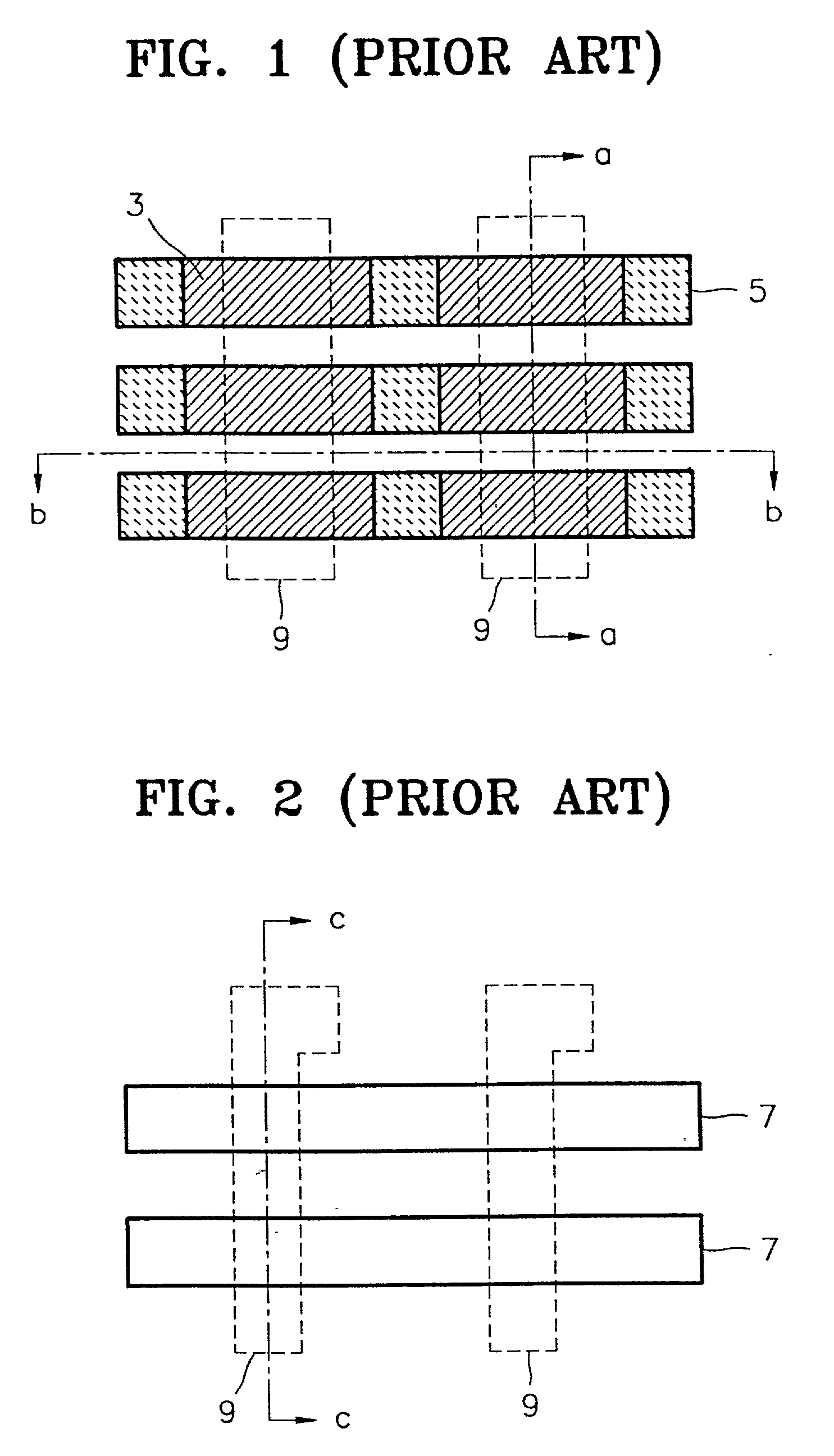
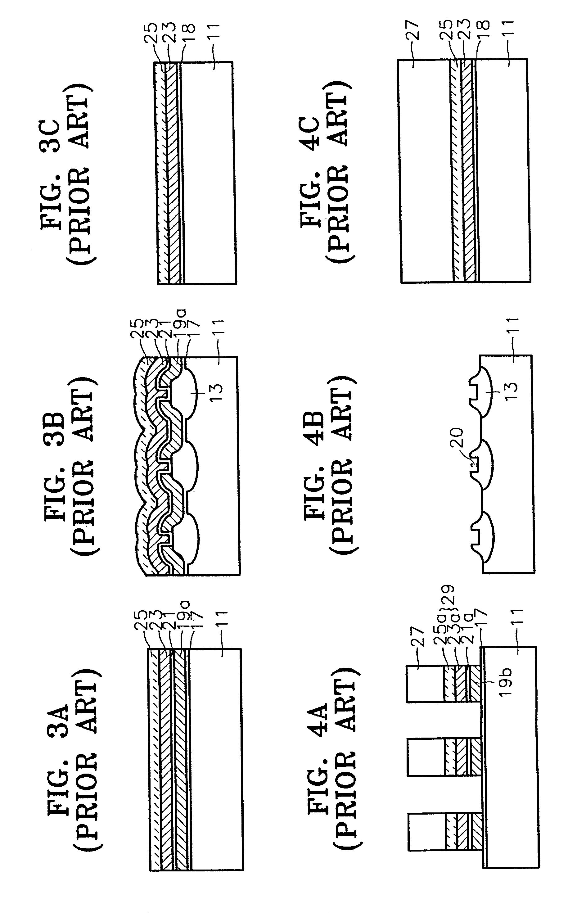
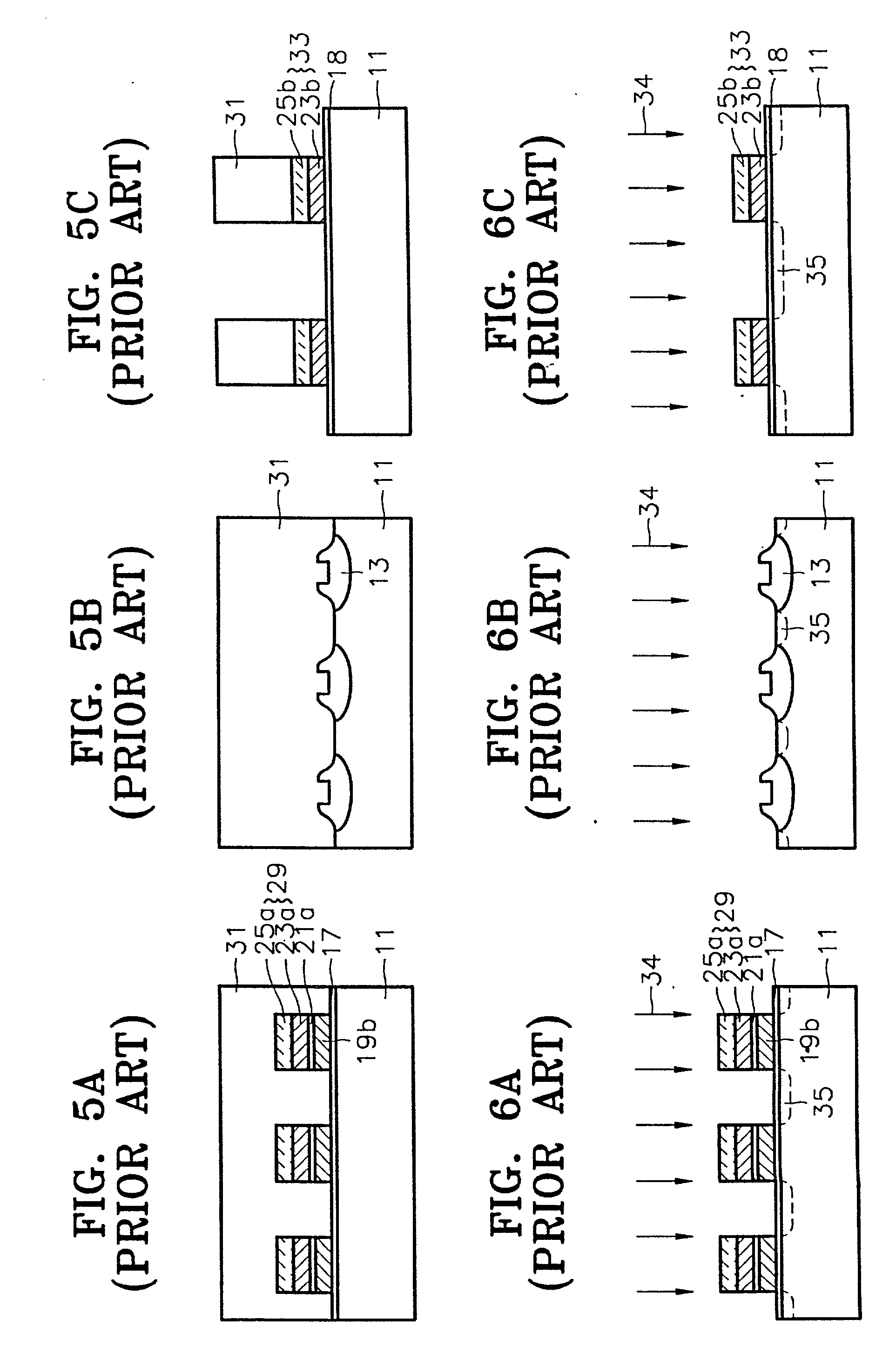
[0037] FIGS. 10A-15A, 10B-15B, and 10C-15C are each sectional views of a nonvolatile semiconductor memory device according to the present invention taken along lines a-a and b-b of FIG. 1 and c-c of FIG. 2, for illustrating the manufacturing method thereof. Referring to FIGS. 10A-10C, a field insulating layer 53 is deposited over a semiconductor substrate 51 to define an active region. Subsequently, a tunnel insulating layer 57 having a thickness of 50-100 .ANG. is formed over the semiconductor substrate 51 of a memory cell array region. The tunnel insulating layer 57 is formed of an oxide layer or a composite layer including oxide and nitride layers. Then, a first conductive layer (not shown) having a thickness of 1,000-1,500 .ANG. such as a polysilicon layer with which group V impurities such as As or P are doped, is provided over the entire surface of the semiconductor substrate 51 on top of which the tunnel insulating layer 57 of the memory cell array region has been formed, and...
second embodiment
[0044] FIGS. 10A-10C are each sectional views of a non-volatile semiconductor memory device according to the present invention taken along lines a-a and b-b of FIG. 1 and c-c of FIG. 2 for explaining a second embodiment of a manufacturing method thereof. In concrete terms, the second embodiment for a manufacturing method of a non-volatile semiconductor memory device is the same as the first one in all aspects other than the manufacturing method for obtaining resultants of FIGS. 10A-10C.
[0045] Referring to FIGS. 10A-10C, a field insulating layer 53 is formed over a semiconductor substrate 51 to define an active region, and then a tunnel insulating layer 57 of 50-100 .ANG. and a first conductive layer (not shown) of 1,000-1,500 .ANG. such as a group V impurity doped polysilicon layer are sequentially provided over the entire surface of the semiconductor substrate 51 including memory cell array and peripheral circuit regions. Next, the first conductive layer is patterned to form a firs...
PUM
 Abstract
Description
Claims
Application Information
 - R&D Engineer
- R&D Manager
- IP Professional
- Industry Leading Data Capabilities
- Powerful AI technology
- Patent DNA Extraction
Browse by: Latest US Patents, China's latest patents, Technical Efficacy Thesaurus, Application Domain, Technology Topic, Popular Technical Reports.
© 2024 PatSnap. All rights reserved.Legal|Privacy policy|Modern Slavery Act Transparency Statement|Sitemap|About US| Contact US: help@patsnap.com


