Method of manufacturing printed wiring board
a manufacturing method and technology of printed wiring, applied in the direction of printed circuit, printed element electric connection formation, chemistry apparatus and processes, etc., can solve the problems of reducing the reliability of interlayer connection, reducing the mechanical strength against pressing force, and reducing the area of the tip end and the lower surfa
- Summary
- Abstract
- Description
- Claims
- Application Information
AI Technical Summary
Problems solved by technology
Method used
Image

Examples
embodiment 1
[0032] Embodiment 1
[0033] In the following, a manufacturing method involving a first embodiment of the present invention will be explained.
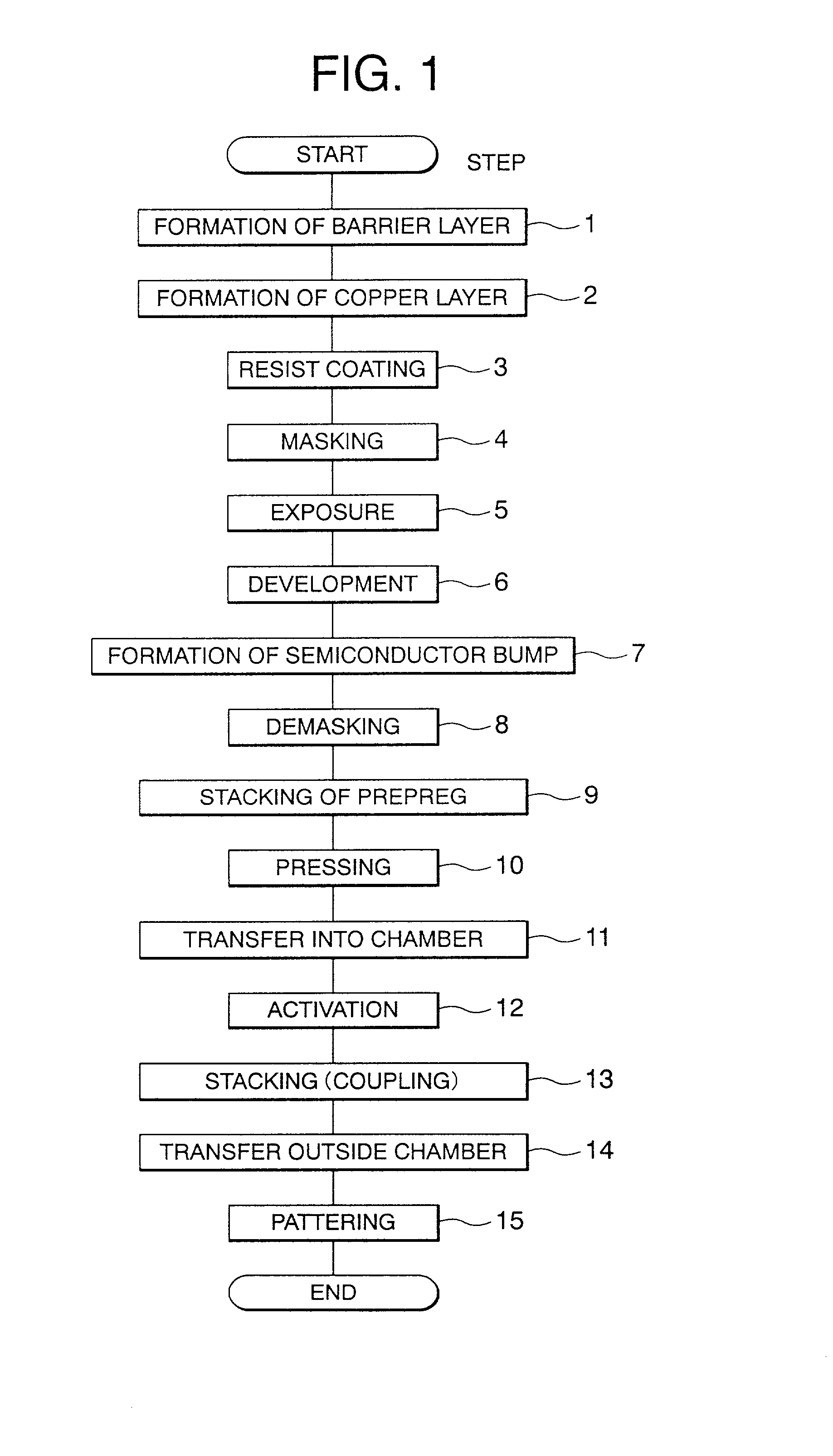
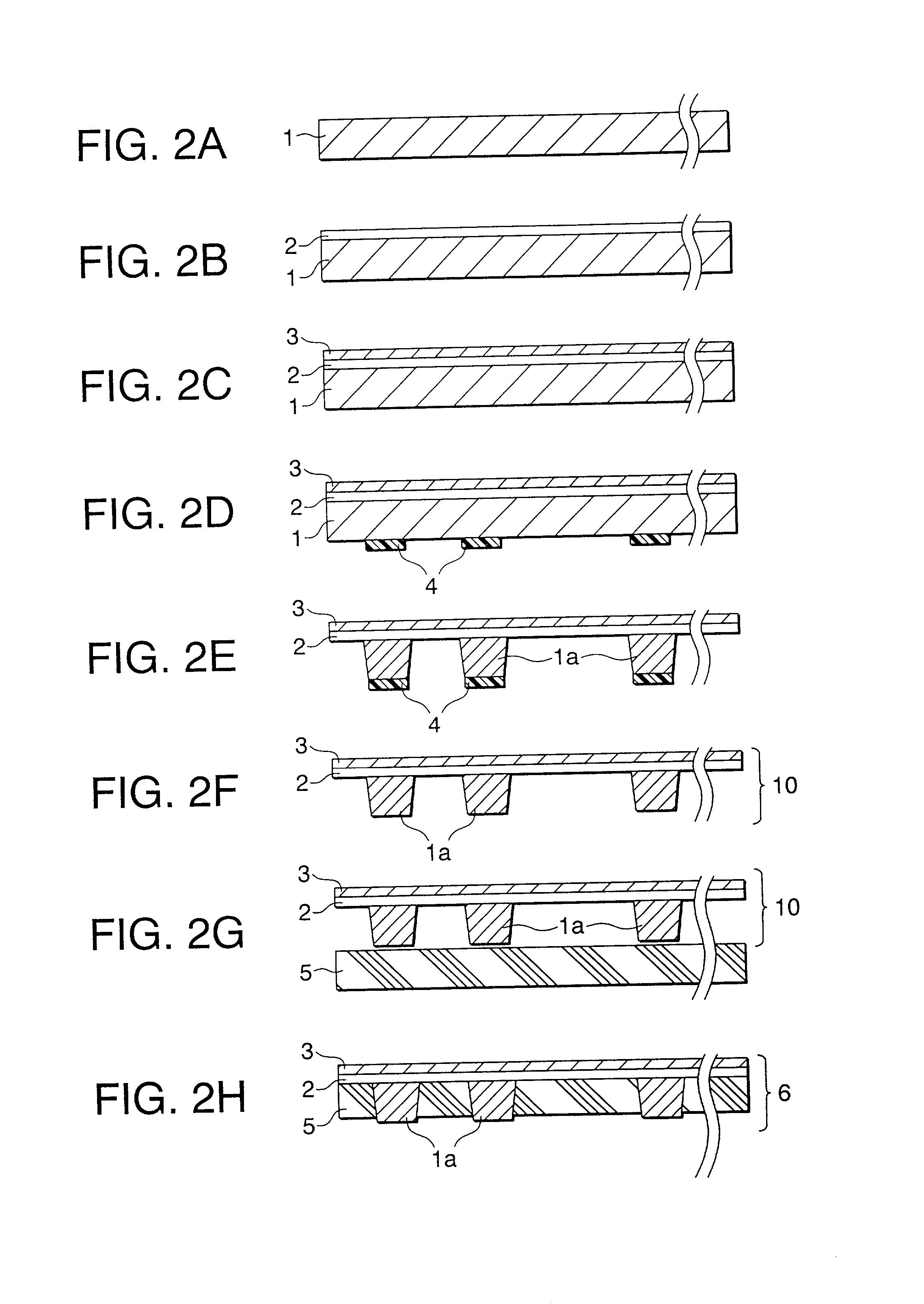
[0034] FIG. 1 is a flow chart illustrating a flow of a manufacturing method of a printed wiring board involving the present embodiment, FIGS. 2 through 7 being vertical sectional views showing schematically the respective steps by which a printed wiring board involving the present embodiment is manufactured.
[0035] For manufacturing a printed wiring board involving the present embodiment, first, a conductor plate 1 such as a thin copper plate or the like as shown in FIG. 2A is prepared. For the conductor plate 1, one of a thickness from 30 to 60 .mu.m is preferably used. The reason for limiting a preferable thickness of the conductor plate 1 to the aforementioned range is as follows. When forming a bump by means of the etching, the size thereof is necessary to have an aspect ratio, a ratio of a lower surface diameter to a height, of approximate 1....
embodiment 2
[0076] Embodiment 2
[0077] In a manufacturing method of a printed wiring board involving the present embodiment, after implementing interlayer connection between a plurality of conductor plates by means of conductor bumps, in gaps between the conductor plates insulating material is filled.
[0078] FIG. 8 is a flow chart illustrating a flow of a manufacturing method of a printed wiring board involving the present embodiment, FIGS. 9 through 15 being vertical sectional views showing schematically each steps by which a printed wiring board involving the present embodiment is manufactured.
[0079] In order to manufacture a printed wiring board involving the present embodiment, a conductor plate 31 such as a thin copper plate as shown in FIG. 9A is prepared, and on one surface of the copper plate 31, a barrier metal layer 32 as shown in FIG. 9B is formed of for instance nickel (step la).
[0080] Then, as shown in FIG. 9C, on the barrier metal layer 32 a copper layer 33 therefrom an interconnect...
PUM
| Property | Measurement | Unit |
|---|---|---|
| Current | aaaaa | aaaaa |
| Temperature | aaaaa | aaaaa |
| Electrical conductor | aaaaa | aaaaa |
Abstract
Description
Claims
Application Information
 - Generate Ideas
- Intellectual Property
- Life Sciences
- Materials
- Tech Scout
- Unparalleled Data Quality
- Higher Quality Content
- 60% Fewer Hallucinations
Browse by: Latest US Patents, China's latest patents, Technical Efficacy Thesaurus, Application Domain, Technology Topic, Popular Technical Reports.
© 2025 PatSnap. All rights reserved.Legal|Privacy policy|Modern Slavery Act Transparency Statement|Sitemap|About US| Contact US: help@patsnap.com