

Semiconductor device and method of manufacturing the same
a semiconductor and semiconductor chip technology, applied in the direction of semiconductor devices, semiconductor/solid-state device details, electrical equipment, etc., can solve the problems of high cost, long time and high cost of the mounting process of the semiconductor chip 8, and the type of semiconductor device that needs radiation of hea
- Summary
- Abstract
- Description
- Claims
- Application Information
AI Technical Summary
Benefits of technology
Problems solved by technology
Method used
Image

Examples
Embodiment Construction
[0022] Hereinafter, the embodiments of the present invention will be explained with reference to the accompanying drawings.
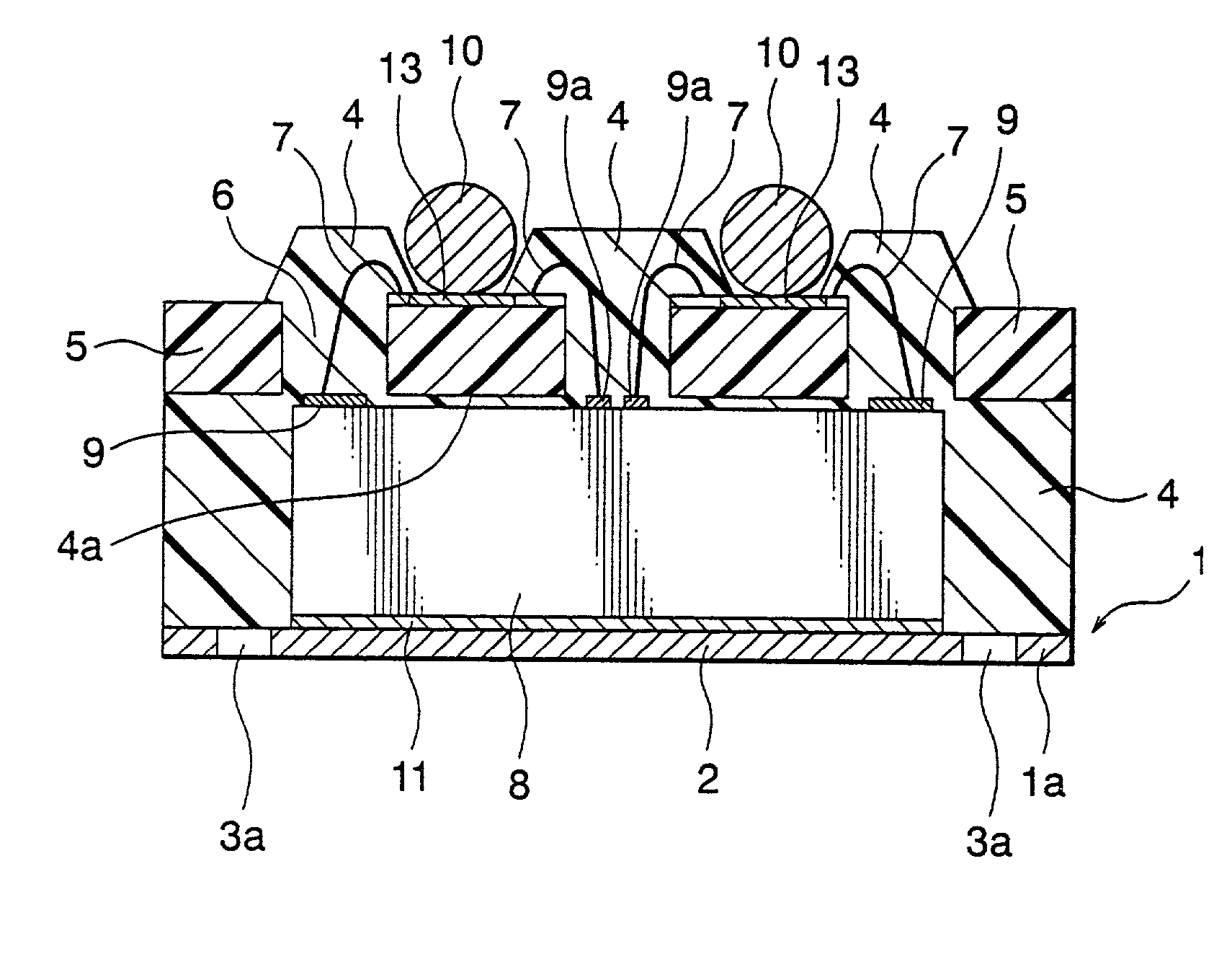
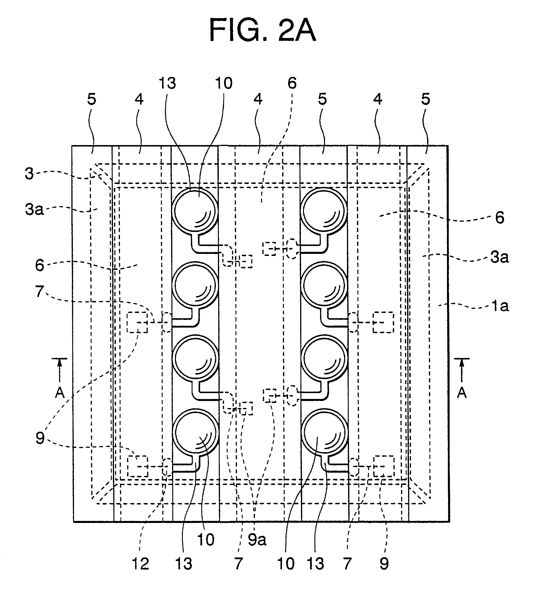
[0023] FIG. 2A is a plan view showing a semiconductor device according to an embodiment of the present invention, FIG. 2B is a cross-sectional view taken by A-A line of FIG. 2A, and FIG. 2C is a partial perspective view excluding a resin body and a resin layer of FIG. 2A. In this semiconductor device, as shown in FIGS. 2A to 2C, a frame member 1 is formed with cut-away portions 3a along four sides. A suspending pin 3 extending from four corners of inner side in an edge 1a to the center thereof is formed by the cut-away portions 3a, and a mounting plate 2 in the center portion is supported by the suspending pin 3. The frame member 1 is made of metal, and a semiconductor chip 8 is mounted on the mounting plate 2 by interposing a bonding metal 11 which is an adhesive. In the semiconductor chip 8, a semiconductor element is formed and electrode pads 9, 9a for transf...
PUM
 Abstract
Description
Claims
Application Information