
Semiconductor device having a ferroelectric capacitor with tensile stress properties

a technology of tensile stress and ferroelectric capacitor, which is applied in the direction of semiconductor devices, capacitors, electrical equipment, etc., can solve the problems of deterioration of the characteristics of the ferroelectric thin film, performance cannot be completely achieved, and the thin film is hard to achiev

Inactive Publication Date: 2002-04-25
JUDAI YUJI
View PDF5 Cites 9 Cited by
  • Summary
  • Abstract
  • Description
  • Claims
  • Application Information

AI Technical Summary

Problems solved by technology

However, the above conventional structure has a disadvantage that characteristics of the ferroelectric thin film are deteriorated and thereby, the performance cannot be completely achieved.
However, when a compression-directional stress is applied to the film, its characteristics are deteriorated.
Therefore, as a result, a semiconductor device in which a ferroelectric thin film is integrated cannot completely show its performances.

Method used


Image

  • Semiconductor device having a ferroelectric capacitor with tensile stress properties
  • Semiconductor device having a ferroelectric capacitor with tensile stress properties
  • Semiconductor device having a ferroelectric capacitor with tensile stress properties

Examples


Embodiment Construction

[0040] Embodiments of the present invention are described below by referring to the accompanying drawings.

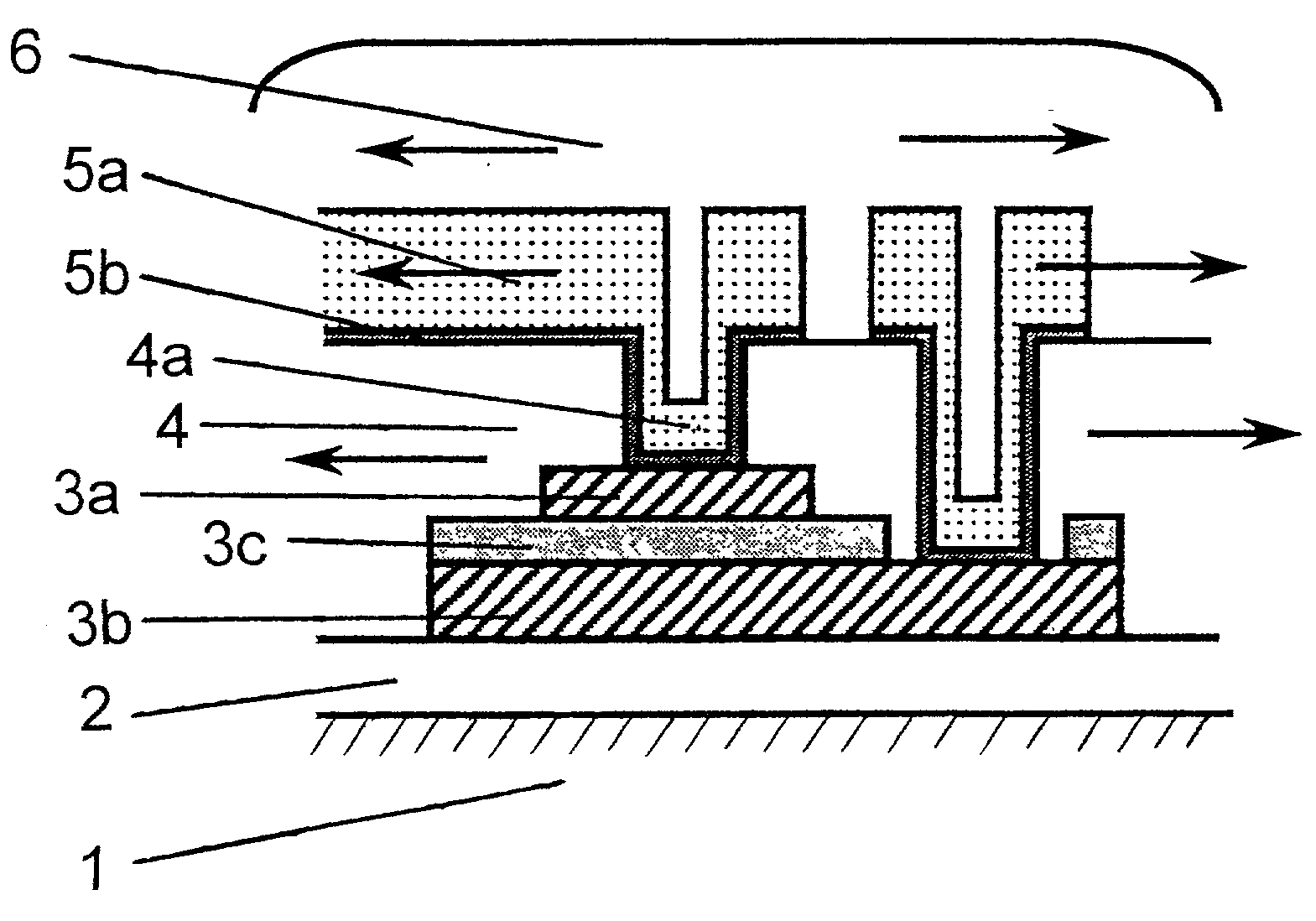
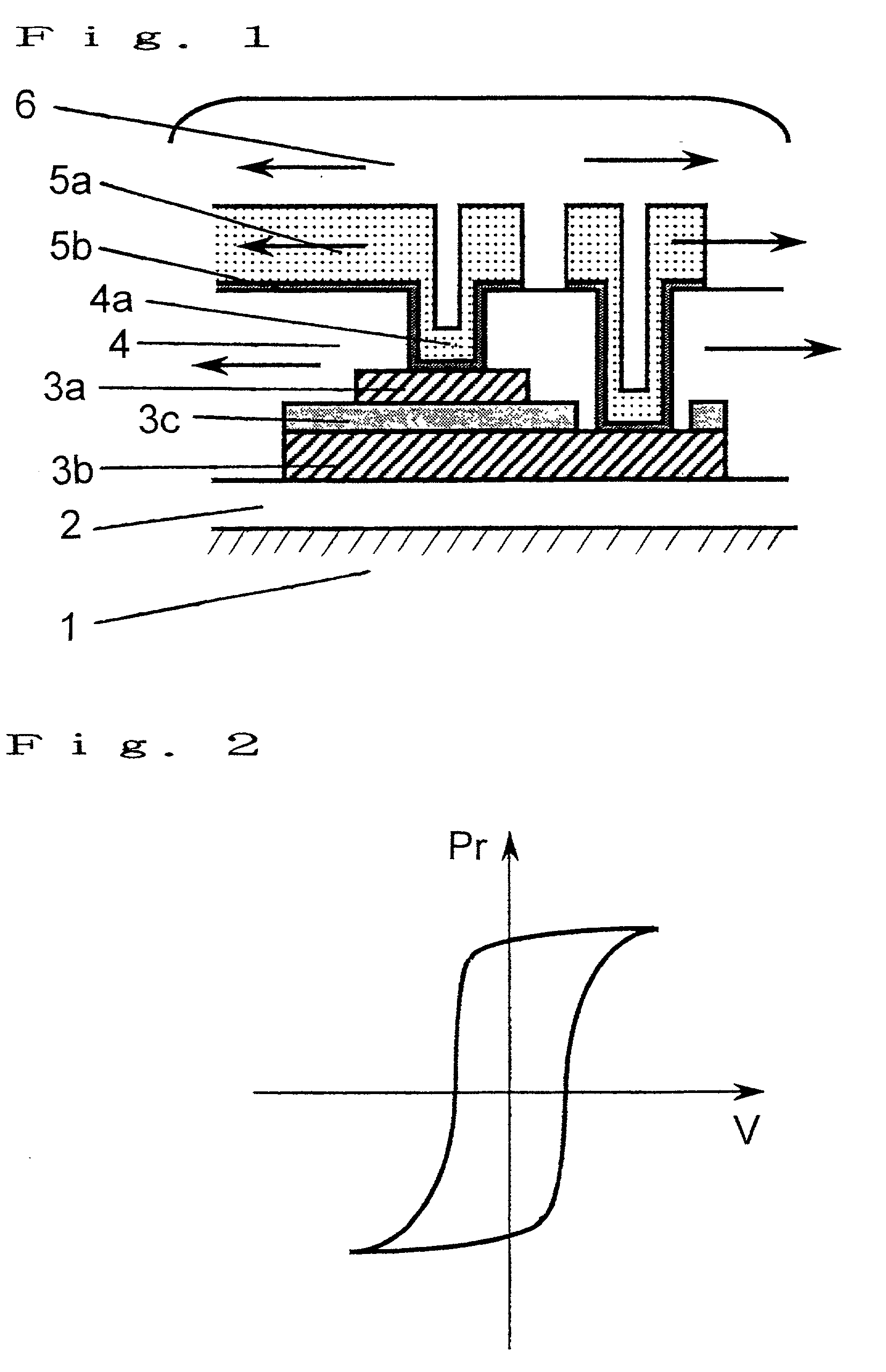
[0041] FIG. 1 shows a sectional view of the ferroelectric capacitor of the semiconductor device of an embodiment of the present invention. In FIG. 1, the ferroelectric capacitor is formed with a top electrode 3a, a bottom electrode 3b, and a ferroelectric thin film 3c on a circuit board 1 comprised of conventional CMOS through an insulating film 2. An insulating film 4 is formed on the ferroelectric capacitor and a CMOS circuit board is connected to wiring films 5a and 5b through a connection hole 4a in the film 4. Moreover, a surface protective film 6 is formed on the wiring films 5a and 5b to protect each element from moisture.

[0042] The semiconductor device of this embodiment is characterized in that the sum of stresses of thin films deposited on the ferroelectric capacitor is an extensional stress. In FIG. 1, arrows show stress directions of thin films. Because the sum of st...


PUM


Abstract

A semiconductor device has a circuit board, a ferroelectric capacitor arranged on said circuit board having a ferroelectric thin film and top and bottom electrodes which are formed so as to hold said ferroelectric thin film, an insulating film formed on said circuit board so as to cover said ferroelectric capacitor, a metallic wiring film formed on said insulating film so as to connect with either of said top and bottom electrodes, and a surface protective film formed so as to cover said insulating film and said metallic wiring film, wherein a synthetic stress working in a surface direction of the ferroelectric thin film of said ferroelectric capacitor is an extensional stress.

Description

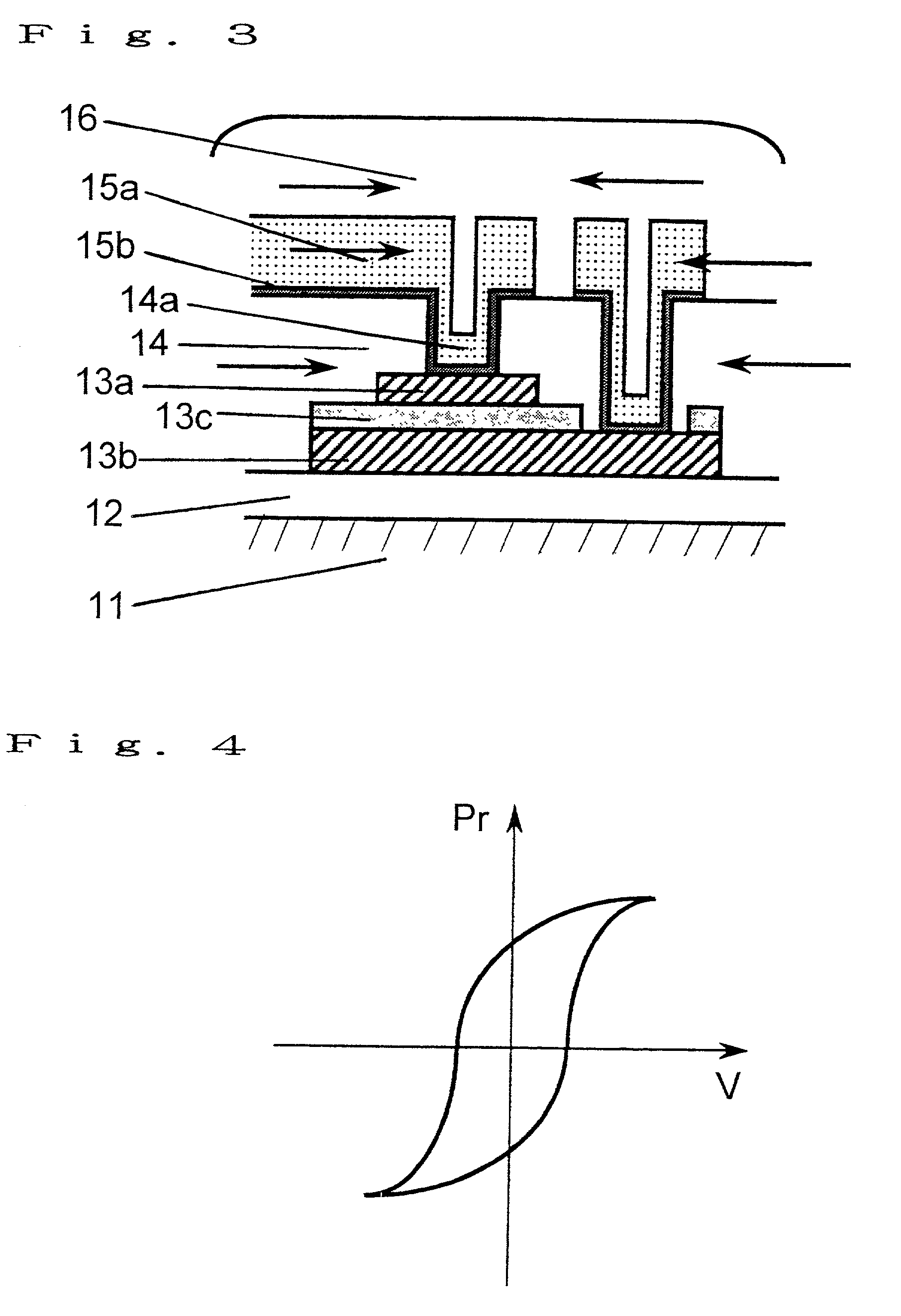
[0001] 1. Field of the Invention[0002] The present invention relates to a semiconductor device, particularly to a nonvolatile memory provided with a ferroelectric capacitor and its fabrication method.[0003] 2. Related Art of the Invention[0004] Recently, an attempt of integrating a capacitor using a ferroelectric thin film in a semiconductor device to obtain a new performance has been positively performed. This is because a ferroelectric thin film has a dielectric constant one place or more higher than that of a conventional silicon oxide film or silicon nitride film and is advantageous for high integration and refining, and moreover the ferroelectric thin film holds electric charges even for a voltage of 0 depending on the material and makes it possible to easily realize a nonvolatile memory.[0005] FIG. 3 shows a sectional view of a semiconductor device in which a ferroelectric capacitor is integrated in accordance with the prior art. In FIG. 3, the ferroelectric capacitor is forme...

Claims


Application Information

Patent Timeline
IPC IPC(8): H01L21/02H01L21/8247H01L21/8242H01L21/8246H01L27/10H01L27/105H01L27/108H01L29/788H01L29/792
CPCH01L28/60
Inventor JUDAI, YUJI
Owner JUDAI YUJI
Learn More