Logical synthesizing apparatus for converting a hardware functional description into gate-level circuit information

a logical synthesizing apparatus and gate-level circuit technology, applied in the field of logical synthesizing apparatuses, can solve the problems of large error between the delay value estimated from the wire load model and the actual delay value, and the timing restrictions satisfied by the wire load model cannot be satisfied, and the wire delay error before and after designing the layout becomes greater

Inactive Publication Date: 2002-04-25
KK TOSHIBA
View PDF0 Cites 17 Cited by
  • Summary
  • Abstract
  • Description
  • Claims
  • Application Information

AI Technical Summary

Problems solved by technology

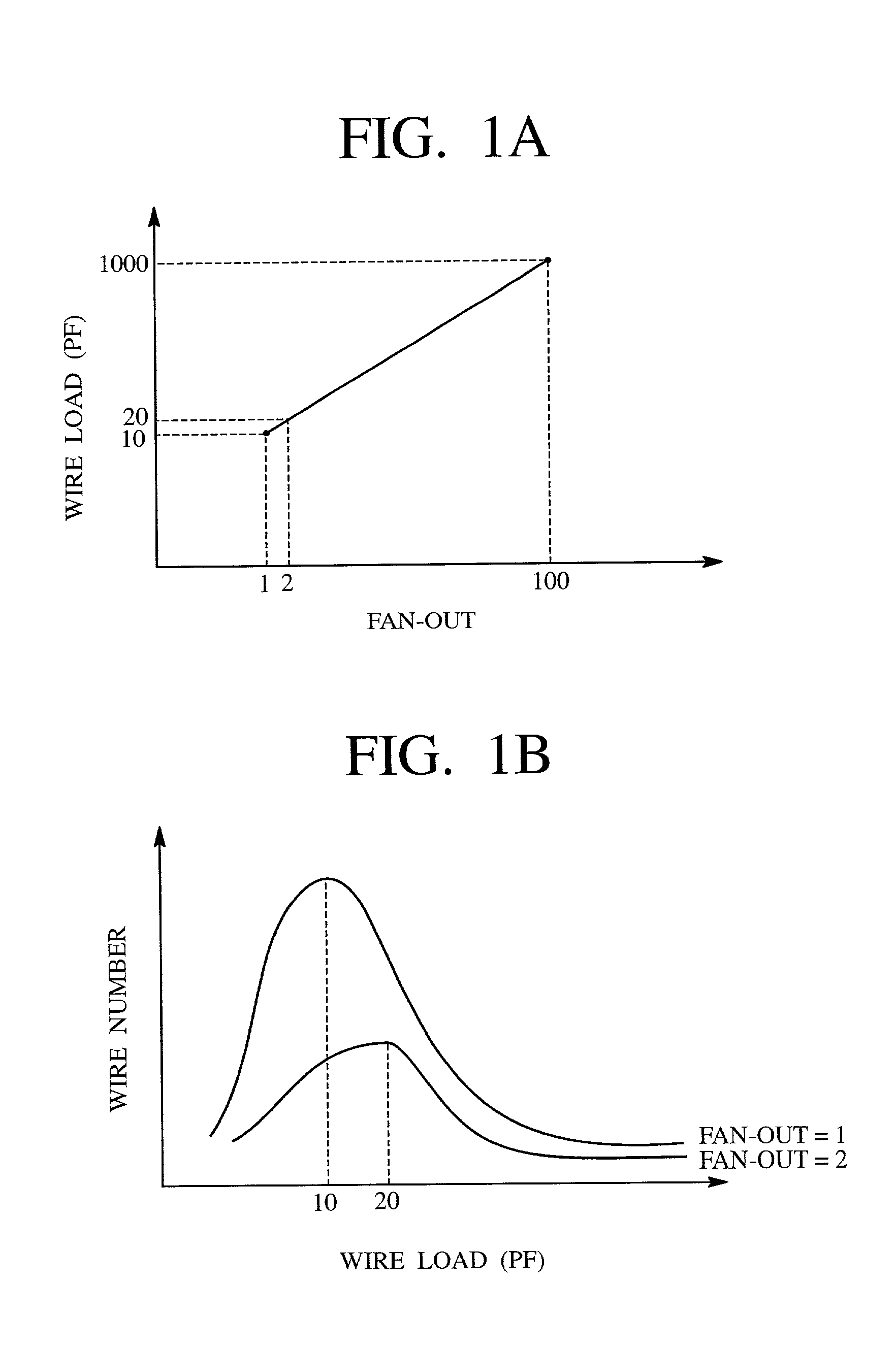
As a result, a great error occurs between a delay value estimated from the wire load model and an actual delay value and timing restrictions satisfied by the wire load model cannot be satisfied after designing a circuit layout.
Further, since the fan-out for the wire to the input pin tends to be 1 and that for the wire to the output pin tends to be 1 to 3, the wire delay error before and after designing the layout becomes greater further.
However, since the functional blocks are logically divided into hierarchies in such processings, it is difficult to eliminate signals transmitted and received among the functional blocks, with the result that many long wires and detoured wires are generated and critical paths are generated.
Third, in the flat layout processing, since the load wire model for the entire chip is employed, respective cells have excessively large driving capabilities, thereby disadvantageously increasing chip area.
Further, if the chip area increases, the dispersion of loads relative to fan-out increases and it is difficult to express wire delay due to long wires and detoured wires using the wire load model, resulting in a large difference in wire delay between before and after layout.
Besides, since the size of the chip

Method used


Image

  • Logical synthesizing apparatus for converting a hardware functional description into gate-level circuit information
  • Logical synthesizing apparatus for converting a hardware functional description into gate-level circuit information
  • Logical synthesizing apparatus for converting a hardware functional description into gate-level circuit information

Examples


Embodiment Construction

[0085] Now, the experimental example of the circuit manufacturing processing in the embodiment according to the present invention will be described with reference to FIGS. 5 to 11 so as to help understand the circuit manufacturing method in the embodiment according to the present invention. It is noted that a circuit having a hierarchical structure shown in FIG. 5 is employed in the description which follows. Namely, this circuit (top) consists of five functional blocks A,B,C,D and E. Each of the functional blocks B and C contains a memory, a macro-cell and two memories. The functional description of the top (first hierarchy) is a connection description for the functional blocks A,B,C,D and E as shown, for example, below:

[0086] module TOP ( . . . );

[0087] input . . .

[0088] output . . . ;

[0089] A A ( . . . )

[0090] B B ( . . . );

[0091] D D ( . . . );

[0092] E E ( . . . );

[0093] endmodule / / TOP

[0094] On the other hand, the functional block A (second hierarchy) consists of four blocks A...


PUM


Abstract

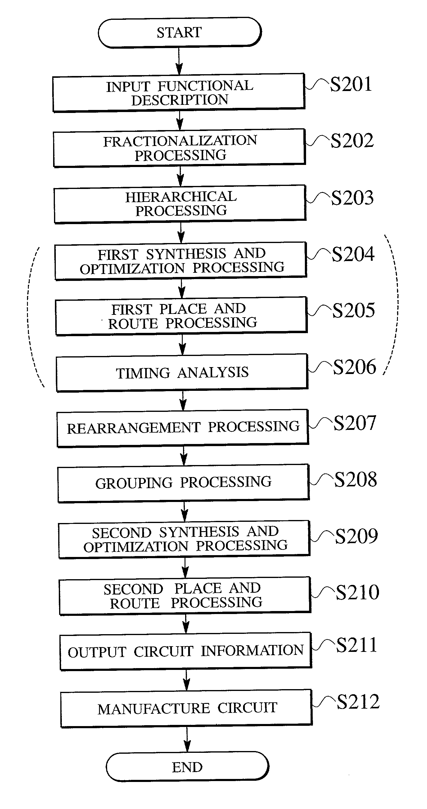
In the disclosed invention, a module in the functional description is fractionalized according to functions, the functional description is converted into two hierarchies and then the fractionalized modules are rearranged so as to decrease a critical path; and the rearranged modules are grouped to generate an intermediate hierarchy and a logical synthesis and optimization processing and a place and route processing are executed using the functional description after the formation of the intermediate hierarchy.

Description

[0001] 1. Field of the Invention[0002] The present invention relates to a logical synthesis apparatus, a logical synthesis method, a logical synthesis program for converting a hardware functional description into gate-level circuit information, and to a circuit manufacturing method for determining a layout in a circuit by conducting a logical synthesis and optimization processing and a layout and route processing to the hardware functional description and for manufacturing a circuit using layout information.[0003] The present invention particularly relates to a technique for converting a hierarchical hardware functional description into a hierarchical structure suited for a layout processing before converting the hierarchical hardware functional description into a gate level by a logical synthesis and optimization processing, thereby suppressing the formation of a critical path and decreasing chip area.[0004] 2. Description of the Related Art[0005] A series of processings for manufa...

Claims


Application Information

Patent Timeline
IPC IPC(8): G06F17/50
CPCG06F17/5068G06F17/5045G06F30/39G06F30/30
Inventor SHIMAZAWA, TAKAYOSHI
Owner KK TOSHIBA
Why Eureka
Try Eureka