Method for manufacturing semiconductor devices having ESD protection

a technology of electrostatic discharge and semiconductor devices, which is applied in the direction of semiconductor devices, diodes, electrical apparatus, etc., can solve the problems of undesired hot electron effect, undesired peak structure of ldd structure, and increased esd stress on scaled-down mos devices and thin gate oxides

Inactive Publication Date: 2002-06-20
SILICON INTEGRATED SYSTEMS
View PDF0 Cites 38 Cited by
  • Summary
  • Abstract
  • Description
  • Claims
  • Application Information

AI Technical Summary

Problems solved by technology

ESD (electrostatic discharge) damage has become one of the main reliability concerns for the IC (integrated circuit) products.
The scaled-down MOS devices and thinner gate oxide have become more vulnerable to ESD stress since the CMOS technology has developed into the sub-quarter-micron regime.
However, the LDD structure can generates an undesired peak structure in the drain region near the surface channel.
However, such method suffers from the undesired hot electron effect and the worst short channel effect while compared to the normal LDD MOSFET structure.
As the ESD current is conducted from the drain contact material to the p substrate, the ESD current discharging through the narrow junction region causes the higher heat which can melt the metal material in the drain contact, resulting in an undesired phenomenon known as "contact spiking".

Method used


Image

  • Method for manufacturing semiconductor devices having ESD protection
  • Method for manufacturing semiconductor devices having ESD protection
  • Method for manufacturing semiconductor devices having ESD protection

Examples


Embodiment Construction

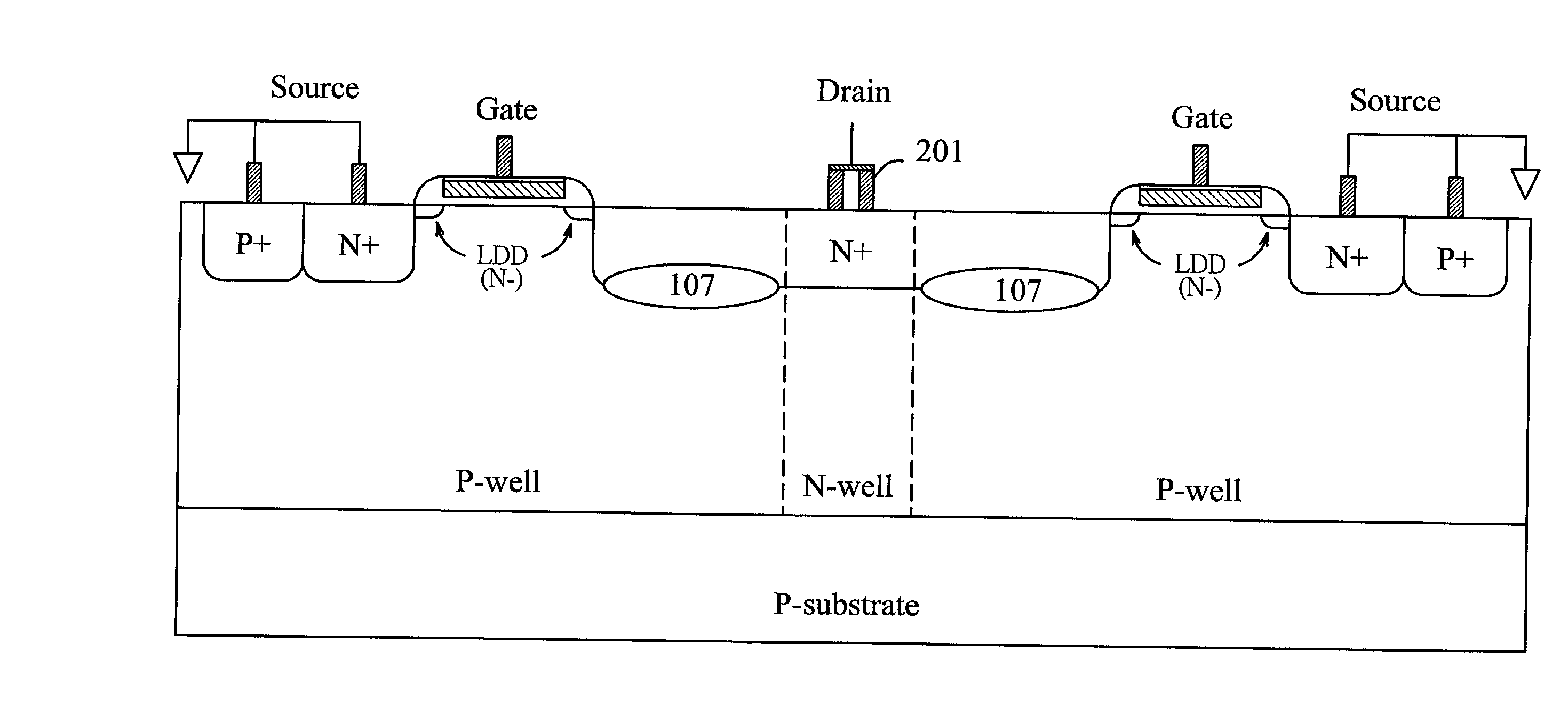
[0029] FIG. 9 illustrates the ESD implantation within an NMOS device and FIG. 10 is the corresponding layout of FIG. 9. According to the first embodiment of the invention, an NMOS with ESD protection includes a gate structure with spacer sidewalls 101, a source region 103 and a drain region 104 beneath a drain contact 102. The LDD (lightly doped drain) regions formed underneath the sidewalls 101 and extending from the source region 103 and drain region 104 respectively is to reduce the hot carrier effect. For example, a typical LDD region is formed by phosphorous implantation or arsenic ion implantation.

[0030] Referring to FIG. 9 and 10, an ESD implantation region 105 with a p-type doping concentration higher than that of the p-well is formed beneath the drain region 104. The layout pattern of the ESD implantation region 105 surrounding the drain contact 102 with respect to the top view as shown in FIG. 10 can be further drawn as a plurality of separated small blocks in parallel to ...


PUM


Abstract

A Method for manufacturing semiconductor devices having ESD protection. The method includes the steps of providing a semiconductor substrate having a well region, forming a gate structure on the semiconductor substrate, the gate structure including an oxide layer, a gate electrode on said oxide layer, and two spacer sidewalls, forming a source region within the well region at one side of the gate structure, forming a drain region within the well region at the other side of the gate structure, forming lightly doped source / drain regions in the well region and beneath the spacer walls of the gate structure wherein the lightly doped source / drain regions have the same conductivity type as the drain region and, and performing an implant with the same conductivity type as the well region as to form an ESD implantation region. The ESD implantation region is located under the diffusion region that is between the drain contact and the poly gate of output NMOS, but without covering the region right under the drain contact. Therefore, the ESD current is discharged through the ESD-implanted region to the substrate without causing current crowding under the drain contact as to burn out the drain contact.

Description

[0001] A. Field of the Invention[0002] The present invention relates to a method for manufacturing semiconductor devices having electrostatic discharge (ESD) protection, and more particularly to an implantation method employing a uniform current distribution for ESD protection.[0003] B. Description of the Related Art[0004] ESD (electrostatic discharge) damage has become one of the main reliability concerns for the IC (integrated circuit) products. The scaled-down MOS devices and thinner gate oxide have become more vulnerable to ESD stress since the CMOS technology has developed into the sub-quarter-micron regime. For general industrial specification, the input and output of the IC products have to sustain the human-body-model ESD stress above 2000 V. Therefore, the ESD protection circuits have to be laid near the input and output pads of the IC to protect the IC from damage.[0005] In the output buffers of CMOS IC's, the output NMOS and PMOS devices are often designed with large devi...

Claims


Application Information

Patent Timeline
Patent Type & Authority Applications(United States)
IPC IPC(8): H01L21/8234H01L27/02H01L29/06H01L29/10
CPCH01L21/823425H01L29/1083H01L29/0692H01L27/0255
Inventor KER, MING-DOULO, WEN-YUHU, PEIR-JY
Owner SILICON INTEGRATED SYSTEMS
Why Eureka
Try Eureka