Interconnect assembly and z-connection method for fine pitch substrates

a technology of interconnection assembly and fine pitch substrate, which is applied in the direction of printed circuit assembling, printed circuit manufacturing, solid-state devices, etc., can solve the problems of reduced integrity of solder joints between pads, low thermal conductivity, and poor heat dissipation ability of solder joints

Inactive Publication Date: 2002-07-11
FUJITSU LTD
View PDF0 Cites 18 Cited by
  • Summary
  • Abstract
  • Description
  • Claims
  • Application Information

AI Technical Summary

Problems solved by technology

The flip-chip bonds provide a good electrical connection, but the solder joints generally exhibit poor heat dissipation capability (low thermal conductivity).
Another disadvantage is that the integrity of the solder joint between the pads can be reduced by thermally induced metal fatigue (differential thermal expansion between the components), and by corrosion caused by trapped solder flux or contaminants.
In addition, because the solder must be heated to a sufficient temperature to cause it to reflow, flip-chip bonding may not be suited for use with some temperature sensitive components (i.e., components which are damaged, or have their electrical characteristics unacceptably altered when heated to solder reflow temperatures).
Wire bonding is a mature technology, however, the wires used in wire bonding are purposefully made very thin, thereby limiting the power they can transfer without failure.
In addition, the lead inductance and resistance of the wires result in a degradation of the electrical performance of the interconnects.
The wires also form a relatively long signal propagation path compared to other interconnect methods, In addition, embrittlement of the interconnections as a result of the formation of intermetallics can cause a failure of the bonds (e.g., this is a problem between gold wirebonds and aluminum pads).
However, like wire bonding, TAB is limited to the interconnection of chips having perimeter I / O pads.
This typically results in a lower overall I / O density than can be obtained using flip-chip technologies.
Finally, because TAB assembly usually requires different tooling for each chip design, TAB is relatively expensive bonding method.

Method used


Image

  • Interconnect assembly and z-connection method for fine pitch substrates
  • Interconnect assembly and z-connection method for fine pitch substrates
  • Interconnect assembly and z-connection method for fine pitch substrates

Examples


Embodiment Construction

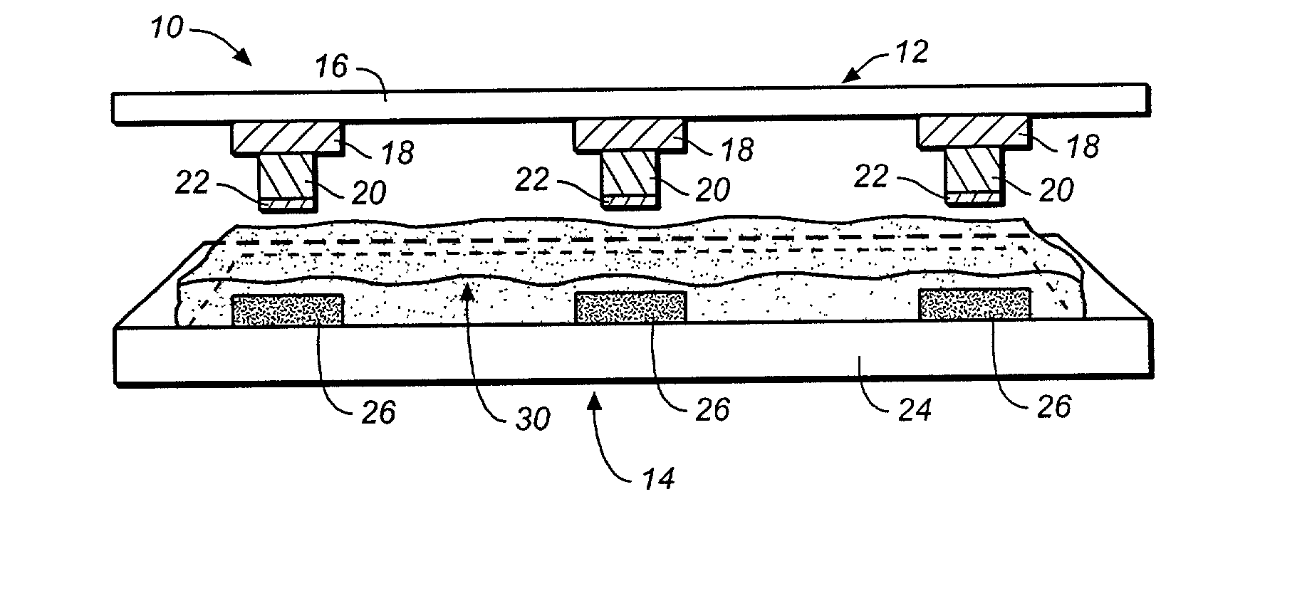
[0020] Referring in detail now to the drawings, there is seen in FIG. 1 a partial perspective segmented view of the interconnect assembly, generally illustrated as 10.

[0021] Interconnect assembly 10 comprises substrate assembly 12 and substrate assembly 14. As best shown in FIG. 2, substrate assembly 12 includes substrate 16, pads 18 secured to the substrate 16, a post 20 secured to each of the pads 18, and a metallic solder 22 mounted to each of the available ends of the posts 20. Substrate assembly 14, as best shown in FIG. 1, includes substrate 24, and pads 26 secured to the substrate 24. A polymer, generally illustrated as 30, is disposed on one of the substrates 16 and 24, preferably substrate 24 as shown in FIG. 1.

[0022] The substrates 16 and 24 may be any suitable substrates which are to be electrically interconnected to form part of the interconnect assembly 10. Suitable substrates include semiconductor substrates, any circuitized substrate, or the like, including suitable e...


PUM

PropertyMeasurementUnit
pressureaaaaaaaaaa
thicknessaaaaaaaaaa
thicknessaaaaaaaaaa

Abstract

An interconnect assembly and a fluxless method for forming the interconnect assembly. The fluxless method includes providing a first semiconductor substrate having a first pad connected thereto. A post is connected to the first pad and includes a length greater than a thickness of the first pad, and a metallic solder disposed on an associated end of the post. A second semiconductor substrate is provided as having a second pad connected thereto. The fluxless method further includes depositing an unfilled polymeric liquid on the second pad, aligning and contacting the metallic solder with the unfilled polymeric liquid, and forcing by pressure the first and second semiconductor substrate toward each while simultaneously heating the metallic solder and the unfilled polymeric liquid to form a metallurgical joint between the second pad and the metallic solder.

Description

[0001] 1. Field of the Invention[0002] The present invention relates to methods of fabricating semiconductor devices. More specifically, embodiments of the present invention provide an interconnect assembly and Z-connection method for coupling together fine pitch substrates.[0003] 2. Description of the Prior Art[0004] Multi-chip modules (MCM) are substrates on which more than one integrated circuit chip is mounted. The substrate (e.g., a chip carrier) typically includes bonding pads for the chip, where the pads may be connected by a set of conductive lines to contact pads for a package or to other bonding pads on the substrate. The conductive lines thus form an interconnect network or I / O path for multiple elements mounted on a common substrate. Although there are other methods for electrically connecting an integrated circuit chip or other component to a substrate, the most commonly used ones are termed flip-chip bonding, wire bonding, and tape automated bonding (TAB).[0005] In fli...

Claims


Application Information

Patent Timeline
Patent Type & Authority Applications(United States)
IPC IPC(8): H05K1/14H01L21/60H05K3/36H05K3/46
CPCH01L24/11H01L24/81H01L2224/13099H01L2224/16H01L2224/81801H01L2224/83192H01L2924/01004H01L2924/01011H01L2924/01013H01L2924/01015H01L2924/01016H01L2924/01018H01L2924/0102H01L2924/01027H01L2924/01029H01L2924/01038H01L2924/01079H01L2924/01082H01L2924/01322H01L2924/01327H01L2924/14H01L2924/30105H01L2924/30107H05K3/4614H05K3/4626H05K2203/0733H05K2203/0759H05K2203/1189H01L2924/01006H01L2924/01033H01L2924/0105H01L2924/014H01L2224/45124H01L2924/00H01L2224/27013H01L2924/00014H01L2224/48H01L2924/3651H01L2224/05568H01L2224/05573H01L2224/13007H01L2224/1308H01L2224/05647
Inventor CHAN, ALBERT W.LEE, MICHAEL G.
Owner FUJITSU LTD
Why Eureka
Try Eureka