Integrated circuits protected against reverse engineering and method for fabricating the same using vias without metal terminations
- Summary
- Abstract
- Description
- Claims
- Application Information
AI Technical Summary
Benefits of technology
Problems solved by technology
Method used
Image
Examples
Embodiment Construction
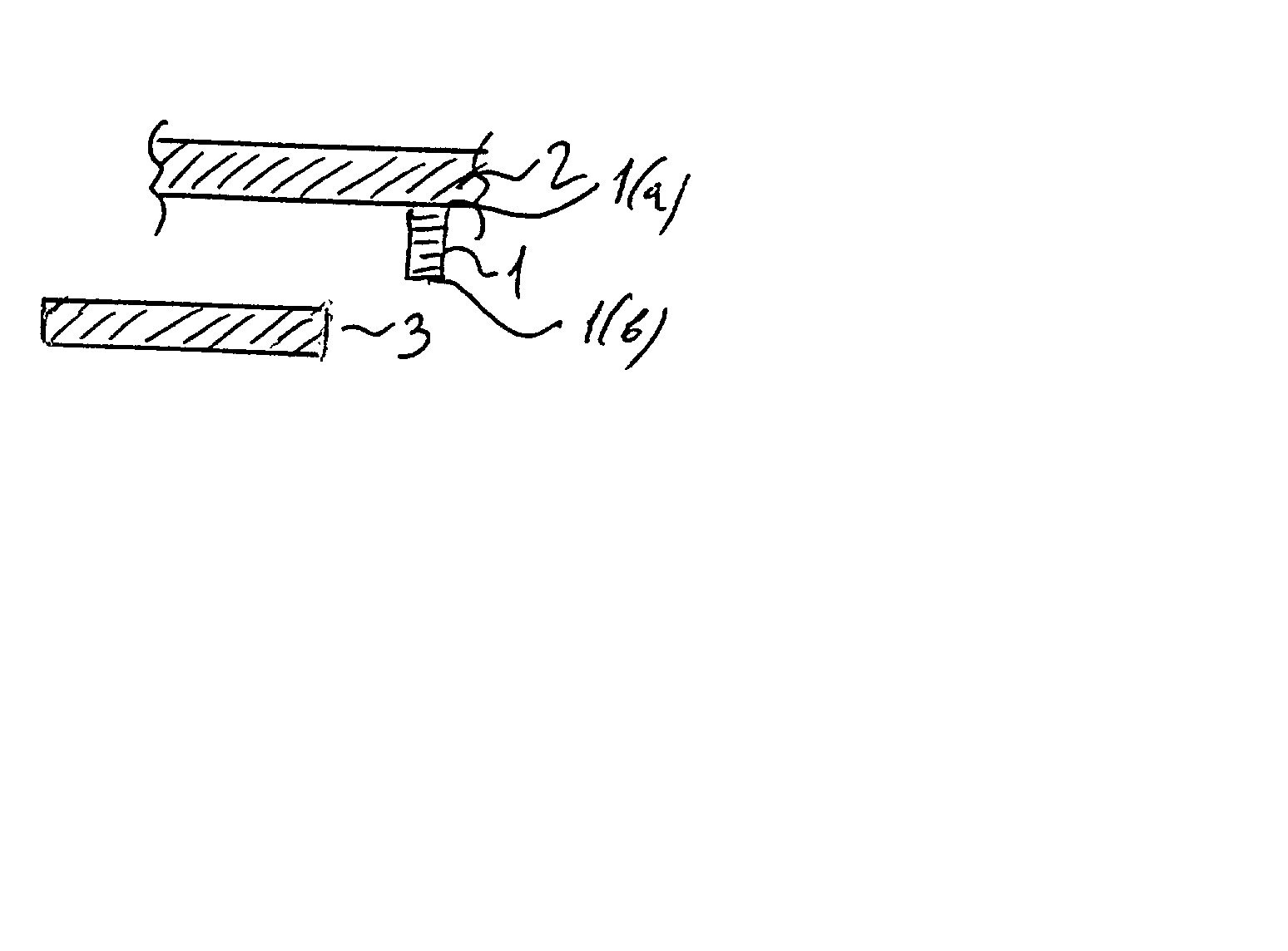
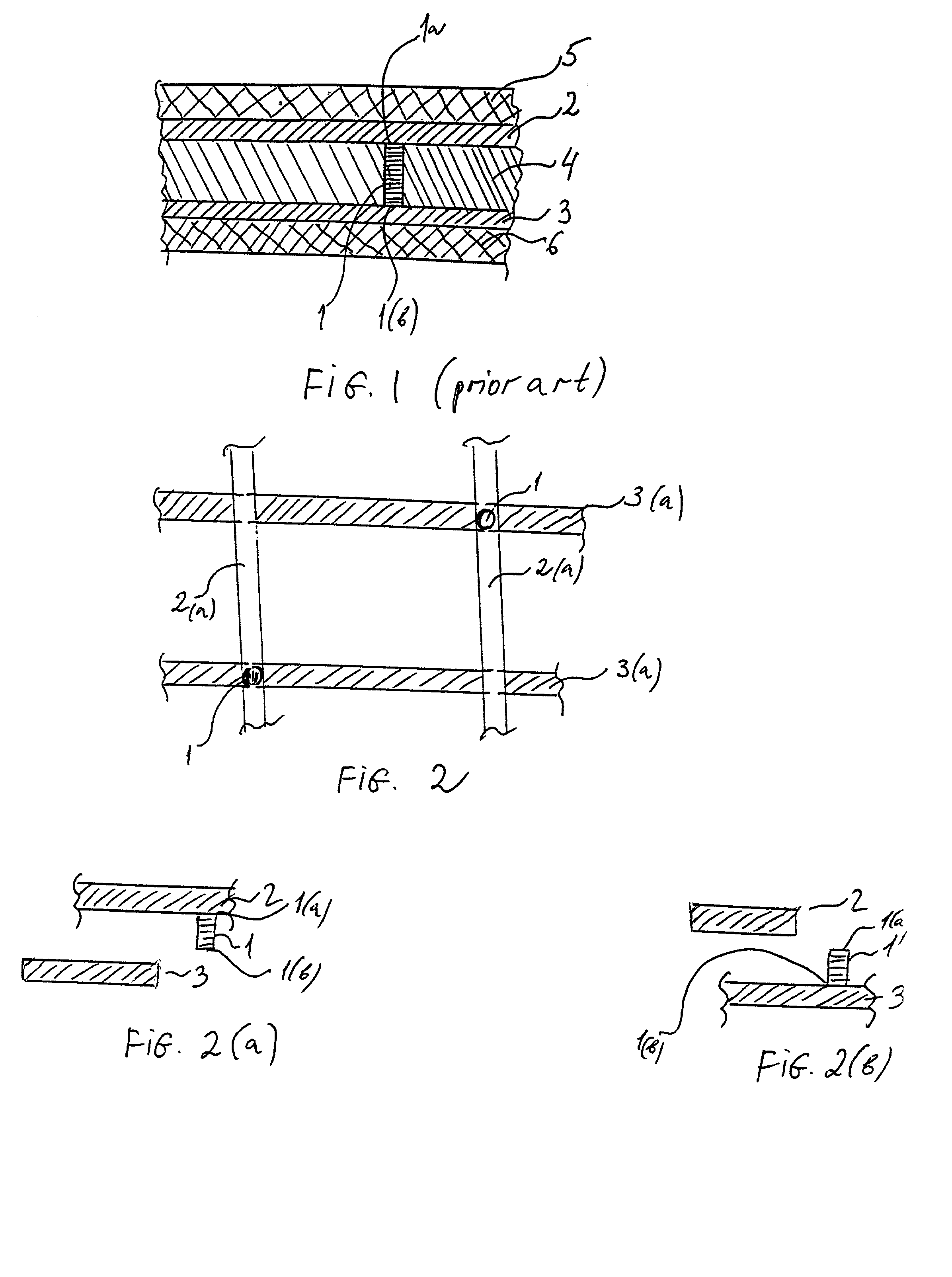
[0030] FIG. 1 shows a usual via 1 connecting an upper metal layer 2 and a lower metal layer 3. The via 1 has two ends: a first end 1(a) and a second end 1(b). The upper and lower metal layers are separated by an insulating layer 4, typically made of silicon oxide. Insulating layers 5 and 6, typically, occur above and below metal layers 2 and 3. The insulating layers 4, 5 and 6 are disposed in a semiconductor device, preferably, an integrated circuit (not shown). The via 1 is filled with a metal, typically the same metal as the metal of metal layers 2 and 3, this metal usually being tungsten.
[0031] FIG. 2 shows that metal lines 2(a) and 3(a), within the two metal layers 2 and 3, respectively, do not typically run parallel. They are disposed in parallel planes, but the signal metal lines 2(a) and 3(a) are not parallel. Instead, the metal pattern, when viewed from the top, as shown on FIG. 2, is usually two arrays of lines proceeding in orthogonal directions, when viewed as projected o...
PUM
 Abstract
Description
Claims
Application Information

