Dielectric filter, dielectric duplexer, and communication device

Inactive Publication Date: 2002-08-15
MURATA MFG CO LTD
View PDF0 Cites 19 Cited by
  • Summary
  • Abstract
  • Description
  • Claims
  • Application Information

AI Technical Summary

Problems solved by technology

As a result, it may occur that the size of a coupling electrode used for capacitive coupling of resonators is reduced and thus a required coupling capacitance may not be obtained.
The required capacitance may be obtained by attaching an external capacitance element, but in that case, problems arise.
For example, the number of components may increase and reliability may be degraded due to the use of solder or the like for connecting the components together.
However, these known die

Method used


Image

  • Dielectric filter, dielectric duplexer, and communication device
  • Dielectric filter, dielectric duplexer, and communication device
  • Dielectric filter, dielectric duplexer, and communication device

Examples


first embodiment

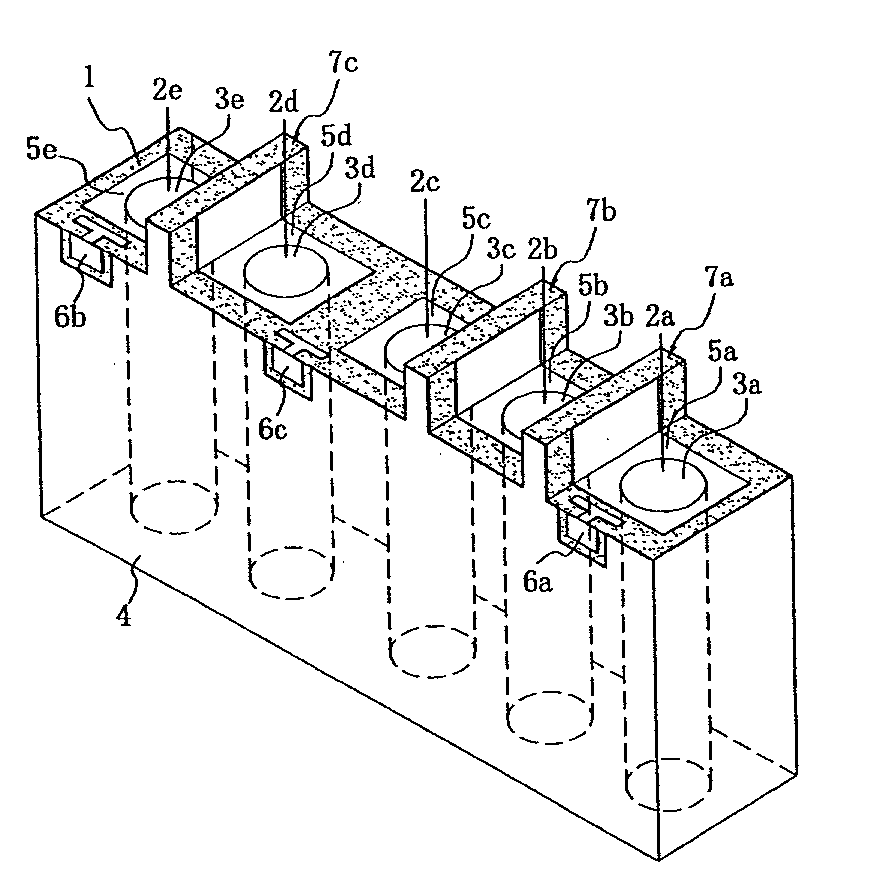
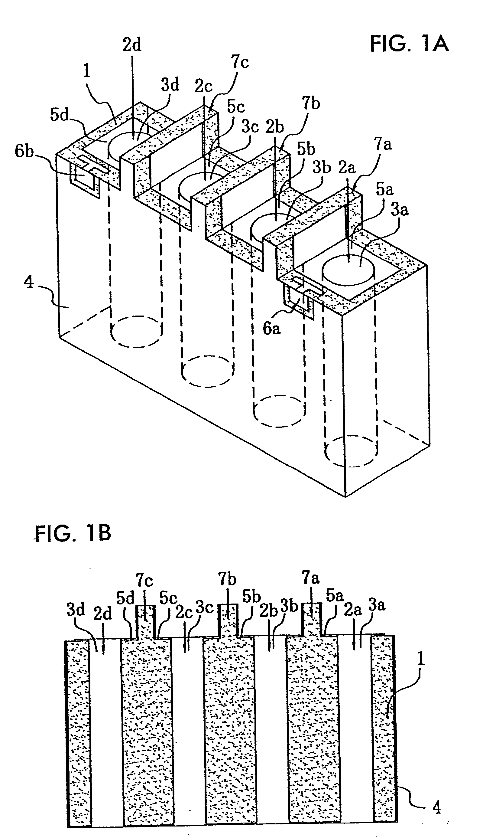
[0031] Hereinafter, the configuration of a dielectric filter is described with reference to FIGS. 1A to 3B.

[0032] FIG. 1A is a perspective view of the dielectric filter and FIG. 1B is a longitudinal sectional view of the same.

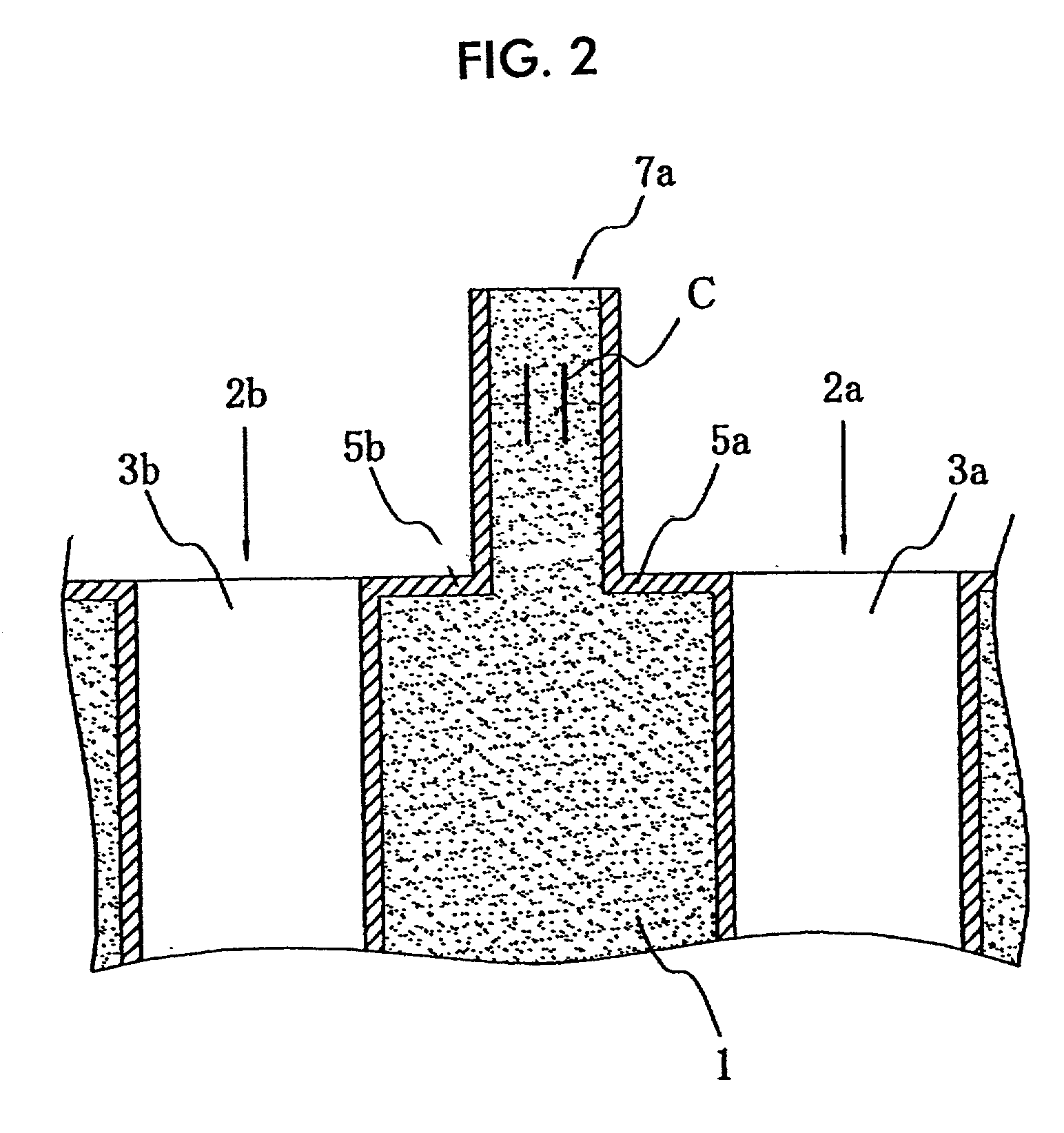
[0033] FIG. 2 is an enlarged longitudinal sectional view of a projection of the dielectric filter.

[0034] FIG. 3A is a perspective view of a dielectric filter according to a modification of the first embodiment and FIG. 3B is a longitudinal sectional view of the same.

[0035] In FIGS. 1A to 3B, the dielectric filter includes a dielectric block 1, innerconductor holes 2a to 2d, inner conductors 3a to 3d, an outer conductor 4, coupling electrodes 5a to 5d, input / output electrodes 6a and 6b, projections 7a to 7c, and a coupling capacitance C.

[0036] As shown in FIGS. 1A and 1B, inside the substantially rectangular parallelepiped dielectric block 1, the inner-conductor holes 2a to 2d having the inner conductors 3a to 3d on the surfaces thereof extend in the direction ...

second embodiment

[0047] Subsequently, the configuration of a dielectric filter is described with reference to FIG. 4.

[0048] FIG. 4 is a perspective view of the dielectric filter.

[0049] In FIG. 4, the dielectric filter includes a dielectric block 1, inner-conductor holes 2a to 2d, inner conductors 3a to 3d, an outer conductor 4, coupling electrodes 5a to 5d, input / output electrodes 6a and 6b, and projections 7a to 7c.

[0050] In the dielectric filter shown in FIG. 4, the projections 7a to 7c are narrower than the shorter edge of a first open surface of the dielectric block 1 and the coupling electrodes 5a to 5d are formed on the entire area of the side surfaces of the projections 7a to 7c. Other than this, the configuration of the dielectric filter is the same as that of the dielectric filter shown in FIGS. 1A and 1B.

[0051] With this configuration, the required coupling capacitance can be obtained with smaller projections, and thus a smaller dielectric filter can be achieved.

third embodiment

[0052] Next, the configuration of a dielectric filter is described with reference to FIG. 5.

[0053] FIG. 5 is a perspective view of the dielectric filter.

[0054] In FIG. 5, the dielectric filter includes a dielectric block 1, inner-conductor holes 2a to 2d, inner conductors 3a to 3d, an outer conductor 4, coupling electrodes 5a to 5d, input / output electrodes 6a and 6b, and projections 7a to 7c.

[0055] Inside the substantially rectangular parallelepiped dielectric block 1, the inner-conductor holes 2a to 2d having the inner conductors 3a to 3d on the surfaces thereof extend in the direction from a first open surface of the dielectric block 1 to the opposite surface. On the outer surface of the dielectric block 1, the outer conductor 4 is formed on five surfaces, that is, all surfaces except the first open surface of the dielectric block 1.

[0056] On the four side surfaces communicating with the first open surface, a portion having no outer conductor formed thereon and having a predeterm...


PUM


Abstract

A dielectric filter includes a dielectric block. A plurality of inner-conductor holes, each having an inner conductor on the surface thereof, extend from a first open surface to the opposing surface through the inside of the dielectric block. On the outer surface of the dielectric block, an outer conductor is formed, except on the first open surface. On the first open surface, projections are provided between respective pairs of inner-conductor holes. Coupling electrodes are formed on the side surfaces of the projections and extending onto the first open surface of the dielectric block, where they connect to the inner conductors. On the outer surface of the dielectric block, input/output electrodes are formed such that they couple to the coupling electrodes.

Description

[0001] 1. Field of the Invention[0002] The present invention relates to a dielectric filter, a dielectric duplexer, and a communication device mainly for use in a microwave band.[0003] 2. Description of the Related Art[0004] A known dielectric filter using a substantially rectangular parallelepiped dielectric block is produced by forming TEM-mode resonators, including a dielectric block, inner conductors, and an outer conductor and by coupling the adjacent resonators to each other.[0005] In recent years, miniaturization of dielectric filters to be mounted in communication devices has been required in accordance with the miniaturization of high-frequency communication devices.[0006] However, in order to miniaturize a dielectric filter itself, each element constituting the dielectric filter is required to be miniaturized accordingly. As a result, it may occur that the size of a coupling electrode used for capacitive coupling of resonators is reduced and thus a required coupling capaci...

Claims


Application Information

Patent Timeline
IPC IPC(8): H01P1/201H01P1/205H01P1/213H04B1/50
CPCH01P1/2056H01P1/2136H01P1/201
Inventor TSUKAMOTO, HIDEKIKURODA, KATSUHITOISHIHARA, JINSEIKATO, HIDEYUKIKITAICHI, YUKIHIRO
Owner MURATA MFG CO LTD
Why Eureka
Try Eureka