Semiconductor device having an organic material layer and method for making the same

a technology of organic materials and semiconductor devices, applied in the direction of semiconductor devices, semiconductor/solid-state device details, electrical apparatus, etc., can solve the problems of reducing the reliance on semiconductor devices, narrowing the pitch of wires, and giving rise to problems

Inactive Publication Date: 2002-09-12
FUJITSU LTD
View PDF0 Cites 36 Cited by
  • Summary
  • Abstract
  • Description
  • Claims
  • Application Information

AI Technical Summary

Benefits of technology

0018] Accordingly, it is a general object of the present invention is to provide a novel and useful semiconductor device and a method for making the same in which one or more of the problems described above are eliminated.

Problems solved by technology

Semiconductor device using wires thus have a tendency that wire pitches become narrower.
If an attempt is made to miniaturize the semiconductor device 1A and achieve a high circuit density, it gives rise to problems.
These disadvantages cause a decline of the reliance of the semiconductor device 1A.
This disadvantage causes a decline of the reliance of the semiconductor device 1B.
Thus, it is difficult to bring the probe pins 18 in contact with all of the projection electrodes 11 properly.
Accordingly, there is a disadvantage that it is impossible to conduct a test with a high reliance.

Method used


Image

  • Semiconductor device having an organic material layer and method for making the same
  • Semiconductor device having an organic material layer and method for making the same
  • Semiconductor device having an organic material layer and method for making the same

Examples


first embodiment

[0075] FIG. 4 is a view showing a semiconductor device 20A according to the present invention. FIG. 5 is a view explaining a method for manufacturing of the semiconductor device 20A.

[0076] Referring to FIG. 4, the semiconductor device 20A is of a so-called chip size package (CSP) type. The semiconductor device 20A includes a semiconductor element 22, a seal resin 24, projection electrodes 23, and an organic material layer 40.

[0077] The semiconductor element 22 has an electrode 25 and an insulting film 27 such as a silicon nitride film. The electrode 25 and the insulting film 27 are formed on a circuit surface 29. A resin film 28 such as a polyimide is formed on an upper part of the insulting film 27. Also, a rewire 26, functioning as an interposer, is formed on the circuit surface 29.

[0078] One end part of the rewire 26 is connected with the electrode 25 through an opening. The opening is formed on an opposite place to the insulting film 27 and the electrode 25 in the resin film 28....

second embodiment

[0099] FIG. 7 is a view showing a semiconductor device 20B according to the present invention. FIG. 8 is a view explaining a method for manufacturing of the semiconductor device 20B.

[0100] In FIGS. 7 and 8, parts that are the same as the parts shown in FIGS. 4 to 6 with respect to the first embodiment are given the same reference numerals in, and explanation thereof will be omitted, as well as the following and other embodiments which will be explained.

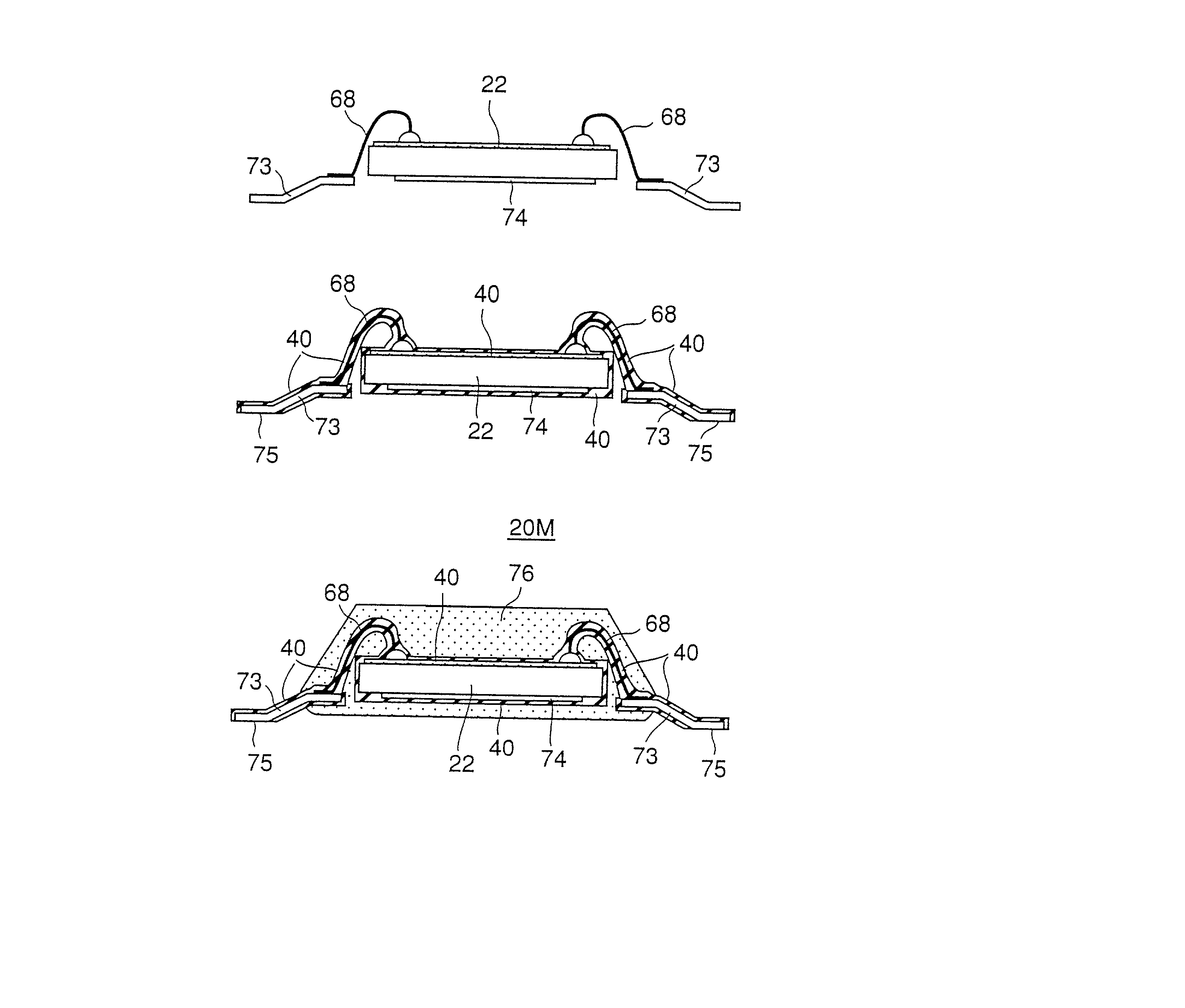
[0101] In the first embodiment, the semiconductor device 20A has a structure in which the organic material layer 40 is arranged on only the back surface 31 and the side surface 32. Contrary, in this embodiment, the semiconductor device 20B has a structure in which the organic material layer 40 is formed on not only the back surface 31 and the side surface 32 but also the connect surface 30.

[0102] The organic material layer 40 is formed on the connect surface 30 except a place where the projection electrode 23 is formed. Accordingly, t...

third embodiment

[0105] FIG. 9 is a view showing a semiconductor device 20C according to the present invention. FIG. 10 is a view showing a method for manufacturing of a semiconductor device 20C.

[0106] In this embodiment, the organic material 40, playing a role of a support member, is not formed on the side surface 32 of the semiconductor device 20C, as shown in FIG. 9. In case of that the handling tool does not contact with the side surface 32, the organic material 40 may not be formed on the side surface 32. Hence, it is possible to reduce the amount of the organic material for use and the cost of the semiconductor device 20C.

[0107] Also, the organic material layer 40 is formed on both the connect surface 30 and the back surface 31. Therefore, warping is prevented from occurring as to the semiconductor device 20C.

[0108] FIG. 10 is a view showing a method for manufacturing of a semiconductor device 20C. As shown in FIG. 10-(A), firstly the projection electrode 23 is formed on the semiconductor subs...


PUM


Abstract

A semiconductor device includes a semiconductor element having a circuit surface on which a projection electrode is formed, a seal resin which seals the circuit surface of the semiconductor element while exposing at least an end part of the projection electrode, a connect surface that is to face a board when the semiconductor device is implemented on the board, a back surface which is opposite to the connect surface, a side surface arranged between the connect surface and the back surface, and an organic material layer formed on the side surface.

Description

BACKGROUND OF THE INVENTION[0001] 1. Field of the Invention[0002] The present invention generally relates to semiconductor devices and methods for making the same, and more particularly, to a semiconductor device having a chip size package structure in which a mold resin is arranged on a semiconductor chip and a method for making the same.[0003] 2. Description of the Related Art[0004] Recently, it has been attempted to miniaturize semiconductor devices and achieve a high circuit density on the basis of a demand for miniaturizing electronic apparatus and devices. Semiconductor device using wires thus have a tendency that wire pitches become narrower. A semiconductor device having a chip size package structure, in which a miniaturization of the semiconductor device is attempted by making a form of the semiconductor device similar to that of a semiconductor chip, has also been proposed.[0005] Against this background, there is a demand for a semiconductor device which can keep high reli...

Claims


Application Information

Patent Timeline
Patent Type & Authority Applications(United States)
IPC IPC(8): H01L23/12H01L21/301H01L21/56H01L21/60H01L23/29H01L23/31
CPCH01L23/293H01L23/3135H01L24/48H01L24/49H01L24/78H01L24/85H01L2224/0401H01L2224/05599H01L2224/274H01L2224/32145H01L2224/48091H01L2224/48145H01L2224/48227H01L2224/48247H01L2224/48465H01L2224/4911H01L2224/78H01L2224/85399H01L2224/8592H01L2924/01004H01L2924/01005H01L2924/01006H01L2924/01014H01L2924/01029H01L2924/01078H01L2924/014H01L2924/12044H01L2924/15311H01L2924/3511H01L2924/00014H01L2224/45099H01L2924/00H01L2224/73265H01L2224/32225H01L2924/181H01L2924/12042H01L2924/00012H01L21/60
Inventor NAKAJO, SHINSUKEFUKASAWA, NORIOHOZUMI, TAKASHINAKASEKO, SHINYA
Owner FUJITSU LTD
Why Eureka
Try Eureka