Wiring board and fabricating method thereof, semiconductor device and fabricating method thereof, circuit board and electronic instrument

Inactive Publication Date: 2002-09-12
ADVANCED INTERCONNECT SYST LTD
View PDF0 Cites 45 Cited by
  • Summary
  • Abstract
  • Description
  • Claims
  • Application Information

AI Technical Summary

Problems solved by technology

However, the process step of filling penetrating holes with a conductive material is often time consuming and troublesome.
A method that forms a film by means such as photolithography and renders the resulting film electrically conductive needs a large number of process steps, a long time and a high cost of production.
A method of filling penetrating holes of a wiring board with a conductive material is also known, but the method needs a long time and troublesome procedures.

Method used


Image

  • Wiring board and fabricating method thereof, semiconductor device and fabricating method thereof, circuit board and electronic instrument
  • Wiring board and fabricating method thereof, semiconductor device and fabricating method thereof, circuit board and electronic instrument
  • Wiring board and fabricating method thereof, semiconductor device and fabricating method thereof, circuit board and electronic instrument

Examples


first embodiment

[0113] First Embodiment

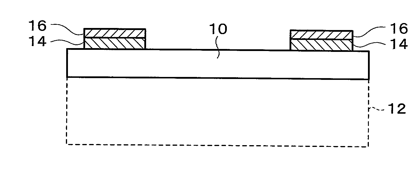
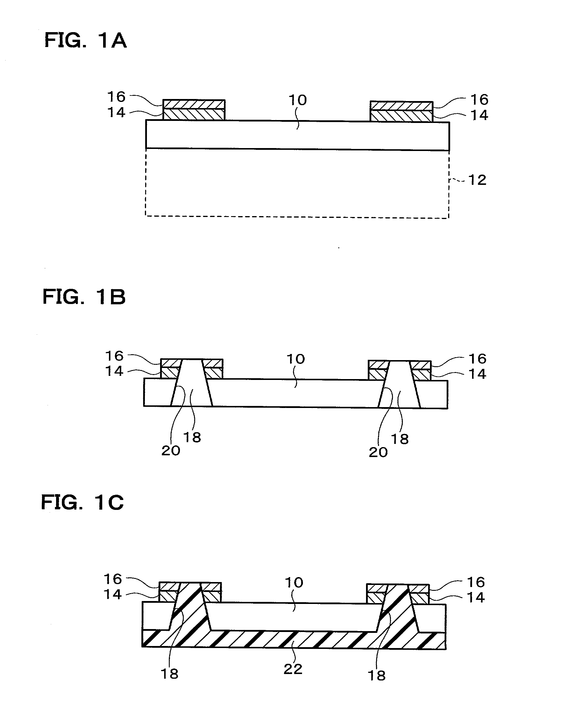
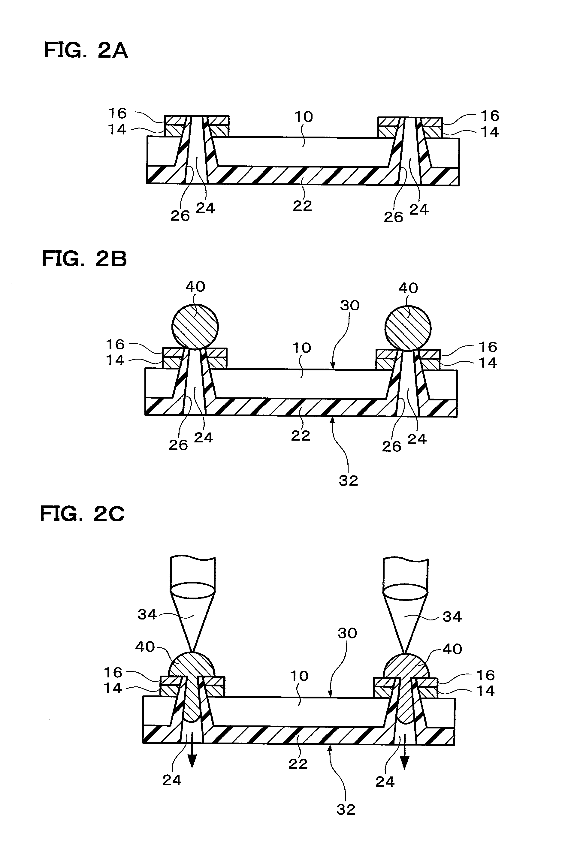
[0114] FIGS. 1A to 2C show a fabrication method of a semiconductor device according to the first embodiment of the invention. FIGS. 3 and 4 show the semiconductor device according to this embodiment. FIGS. 5 to 7 show a semiconductor device and a production method according to modifications of this embodiment. First, penetrating holes 24 are formed in such a fashion as to penetrate through at least a semiconductor chip 10 as shown in FIGS. 1A to 2A.

[0115] As shown in FIG. 1A, the semiconductor chip 10 (semiconductor device) is prepared. The semiconductor chip 10 is a rectangle in most case, but its shape is not limited and may be a sphere, for example. The semiconductor chip 10 may be cut to a thickness smaller than that of its original semiconductor chip 12 (or a semiconductor wafer). More specifically, the surface of the semiconductor chip 10 that is opposite to the surface on which an integrated circuit (not shown) is to be formed (active surface) is cut. C...

second embodiment

[0155] Second Embodiment

[0156] FIGS. 8A to 8C show a fabrication method of a semiconductor device according to the second embodiment of the invention. The technical content of the first embodiment can be applied as much as possible to this embodiment. In this embodiment, a conductive material 140 is made to flow into penetrating holes 24 of a semiconductor wafer 110.

[0157] As shown in FIG. 8A, the semiconductor wafer 110 (semiconductor chip) is first prepared. The semiconductor wafer 110 has a plurality of penetrating holes 24. The form and the formation method of the penetrating holes 24 of the foregoing examples can be applied.

[0158] The conductor material 140 is placed on the first surface 30 of the semiconductor wafer 110 above the penetrating holes 24 as shown in FIG. 8B. The conductor material 140 is paste-like such as a solder paste. The conductor material 140 may be applied by means such as a screen-printing system and application by using a dispenser. Particularly when the ...

third embodiment

[0166] Third Embodiment

[0167] FIGS. 9A to 9C show a fabrication method of a semiconductor device according to the third embodiment of the present invention. The technical content of the first and second embodiments can be applied as much as possible to this embodiment. In this embodiment, a conductive material 40 is provided in penetrating holes 66 of a board 60.

[0168] A board 60 is first prepared as shown in FIG. 9A. The board 60 may be made of an organic material (resin type) or an inorganic material (ceramic type, metal type) or their composite system. The board 60 may use a glass epoxy board or a polyimide board, for example. The overall shape of the board 60 is not limited, but is in most cases similar to the planar shape of the semiconductor chip 10. The thickness of the board 60 is decided in accordance with its material and is not particularly limited. The board 60 may have a single layer or multiple layers.

[0169] An interconnecting pattern 62 is formed on the board 60. The ...


PUM


Abstract

A conductive material is provided to an open end of a penetrating hole penetrating through at least a semiconductor element, on the side of a first surface of the semiconductor element. The conductive material is melted to flow into the penetrating hole. The conductive material is made to flow into the penetrating hole in a state that an atmospheric pressure on the side of a second surface of the semiconductor element opposite to the first surface is lower than an atmospheric pressure on the side of the first surface.

Description

[0001] Japanese Patent Application No. 63650 / 2001 filed on Mar. 7, 2001, is hereby incorporated by reference in its entirety.BACKGROUND OF THE INVENTION[0002] This invention relates to a wiring board and a fabricating method thereof, a semiconductor device and a fabricating method thereof, a circuit board and an electronic instrument.[0003] A form that electrically connects both surfaces of a semiconductor chip by boring penetrating holes in the semiconductor chip, forms an insulating film and then forms either wet or dry an electrically conductive film, or filling penetrating holes with molten solder is known. Since this method eliminates the necessity for disposing wires, a compact semiconductor device can be acquired even when a plurality of semiconductor chips is stacked one upon another.[0004] However, the process step of filling penetrating holes with a conductive material is often time consuming and troublesome. A method that forms a film by means such as photolithography and...

Claims


Application Information

Patent Timeline
IPC IPC(8): H05K1/11H01L21/60H01L21/768H01L23/12H01L23/48H01L25/065H01L25/07H01L25/10H01L25/11H01L25/18H05K1/14H05K3/34H05K3/40
CPCH01L21/486H01L21/76882H01L21/76898H01L23/481H01L24/03H01L24/05H01L24/11H01L24/13H01L24/16H01L24/81H01L25/0657H01L25/50H01L2224/0345H01L2224/0401H01L2224/051H01L2224/05563H01L2224/05567H01L2224/0557H01L2224/05572H01L2224/056H01L2224/1132H01L2224/11334H01L2224/1134H01L2224/1181H01L2224/11849H01L2224/13009H01L2224/1319H01L2224/13411H01L2224/13444H01L2224/13483H01L2224/16146H01L2224/16227H01L2224/16237H01L2224/17181H01L2224/811H01L2224/81191H01L2224/81193H01L2224/814H01L2224/8149H01L2224/81815H01L2224/8185H01L2225/06513H01L2225/06517H01L2225/06541H01L2225/06565H01L2924/01013H01L2924/01029H01L2924/01047H01L2924/01079H01L2924/09701H01L2924/1016H01L2924/1017H05K3/3494H05K3/4038H05K2201/0305H05K2201/096H05K2203/041H05K2203/082H05K2203/107H01L2924/0105H01L2924/014H01L2224/9202H01L2924/01005H01L2924/01006H01L2924/01033H01L2924/01075H01L2924/0002H01L2224/05552H01L2224/16225H01L2924/12042H01L2924/00H01L2924/14
Inventor UMETSU, KAZUSHIGEKURASHIMA, YOHEIAMAKO, JUN
Owner ADVANCED INTERCONNECT SYST LTD
Why Eureka
Try Eureka