

Lead frame laminate and method for manufacturing semiconductor parts
a technology of lead frame laminate and semiconductor parts, which is applied in the direction of film/foil adhesives, transportation and packaging, chemistry apparatus and processes, etc., can solve the problems of increased time for manufacturing/delivery, increased number of steps, and increased harmful effects, and achieve the effect of reducing the quantity of silicone residues
- Summary
- Abstract
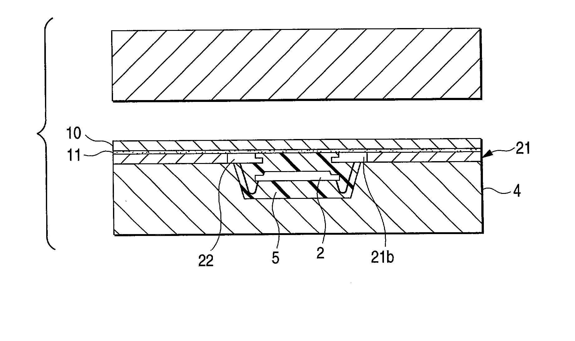
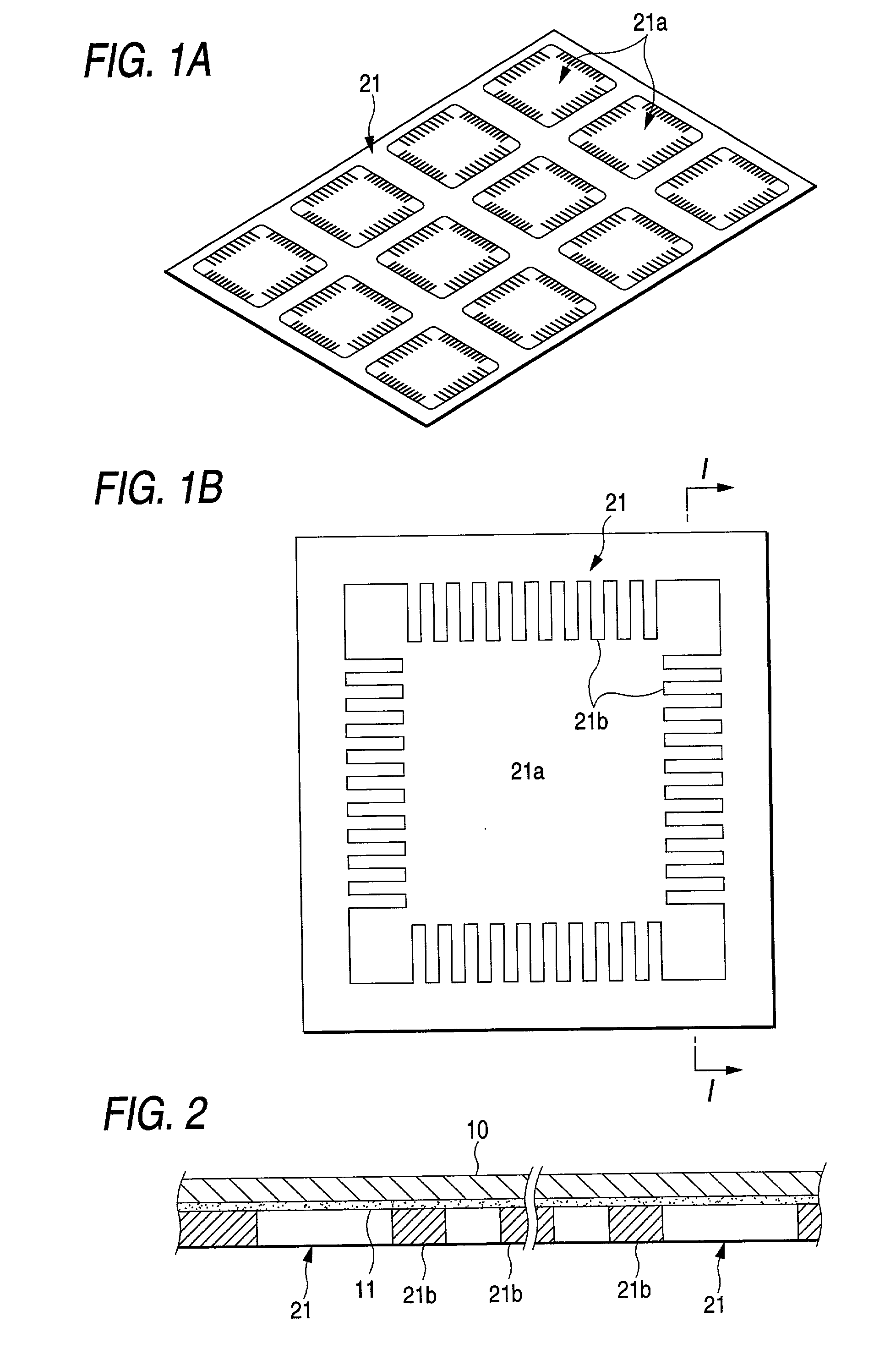
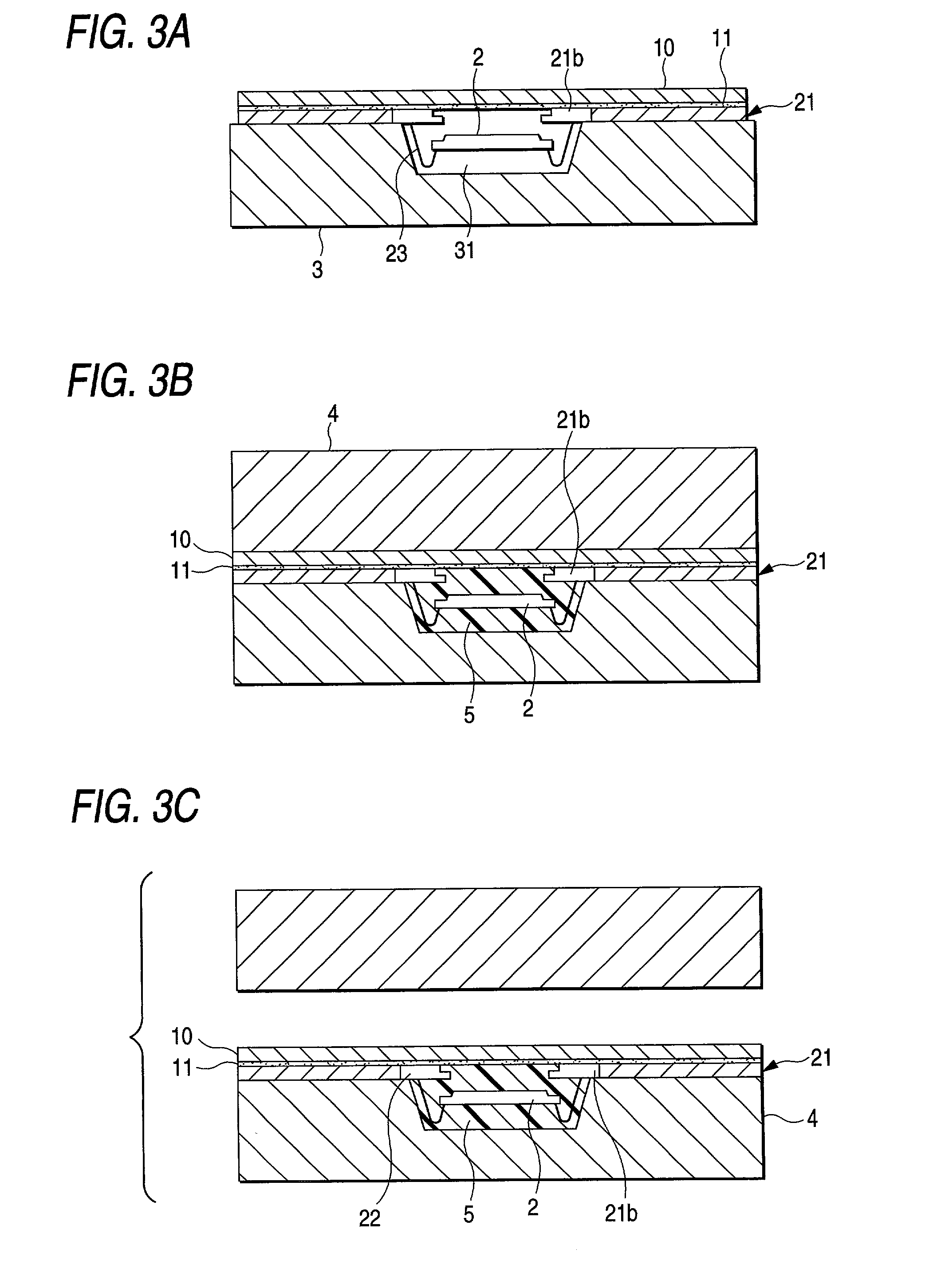
- Description
- Claims
- Application Information
AI Technical Summary
Benefits of technology
Problems solved by technology
Method used
Image

Examples
example 2
[0044] Conditions were set to be similar to those in Example 1, except that the quantity of the hindered phenol oxidation inhibitor (IRGANOX1010) was set to be 5 parts by weight. Thus, a lead frame laminate was obtained, and then the respective estimates were carried out similarly.
example 3
[0045] Conditions were set to be similar to those in Example 1, except that the quantity of the hindered phenol oxidation inhibitor (IRGANOX1010) was set to be 10 parts by weight. Thus, a lead frame laminate was obtained, and then the respective estimates were carried out similarly.
example 4
[0046] Conditions were set to be similar to those in Example 1, except that IRGANOX1330 was used as the hindered phenol oxidation inhibitor. Thus, a lead frame laminate was obtained, and then the respective estimates were carried out similarly.
PUM
| Property | Measurement | Unit |
|---|---|---|
| Fraction | aaaaa | aaaaa |
| Percent by mass | aaaaa | aaaaa |
| Percent by mass | aaaaa | aaaaa |
Abstract
Description
Claims
Application Information