Organic semiconductor devices with short channels

a technology of organic semiconductors and channels, applied in the direction of solid-state devices, transistors, basic electric elements, etc., can solve the problems of disappearing several problems arising in circuits based on organic fets

Inactive Publication Date: 2002-11-21
LUCENT TECH INC
View PDF0 Cites 42 Cited by
  • Summary
  • Abstract
  • Description
  • Claims
  • Application Information

AI Technical Summary

Problems solved by technology

If these two characteristics had values closer to those of inorganic FETs, several problems arising in circuits based on organic FETs would disappear.

Method used


Image

  • Organic semiconductor devices with short channels
  • Organic semiconductor devices with short channels
  • Organic semiconductor devices with short channels

Examples


Embodiment Construction

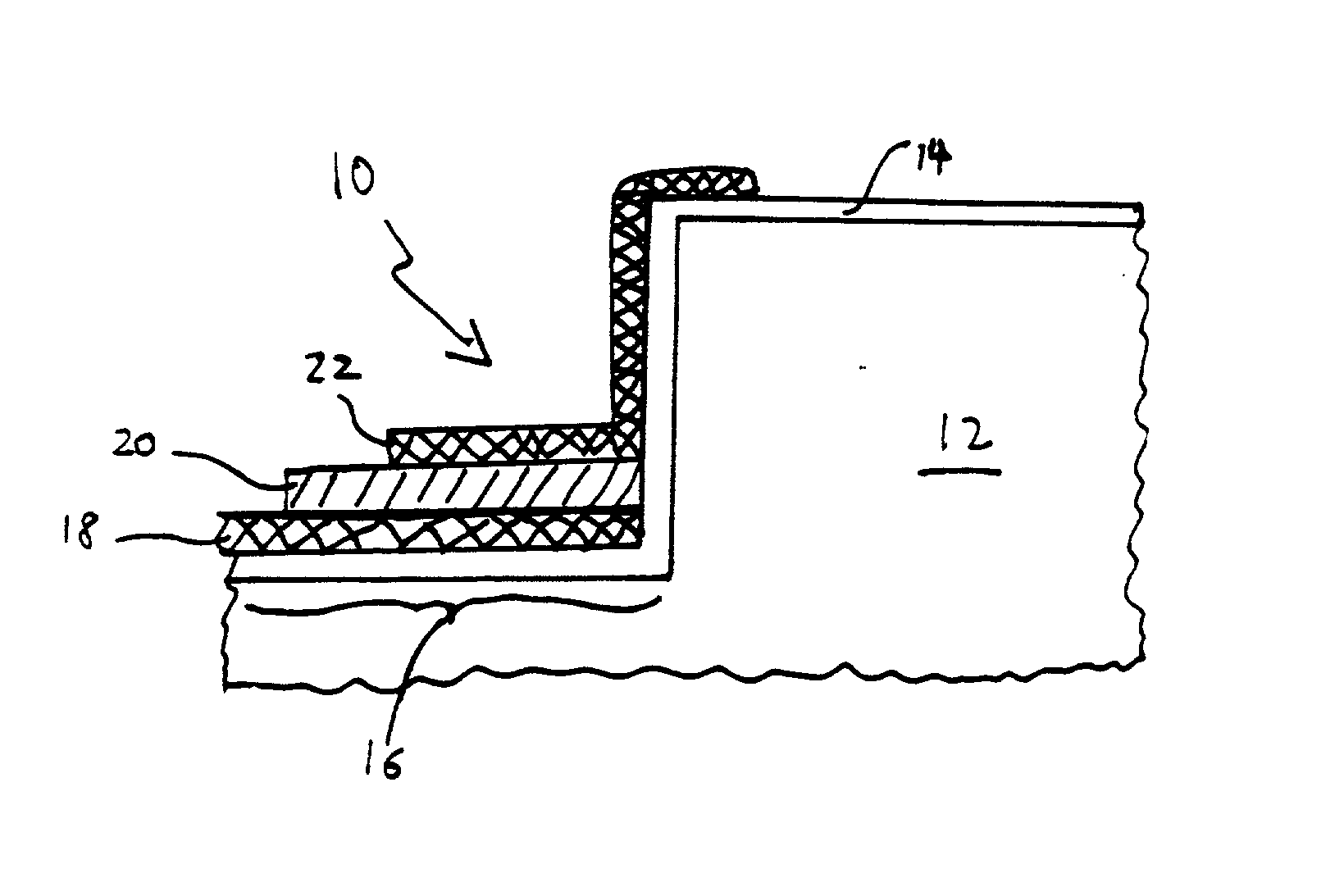
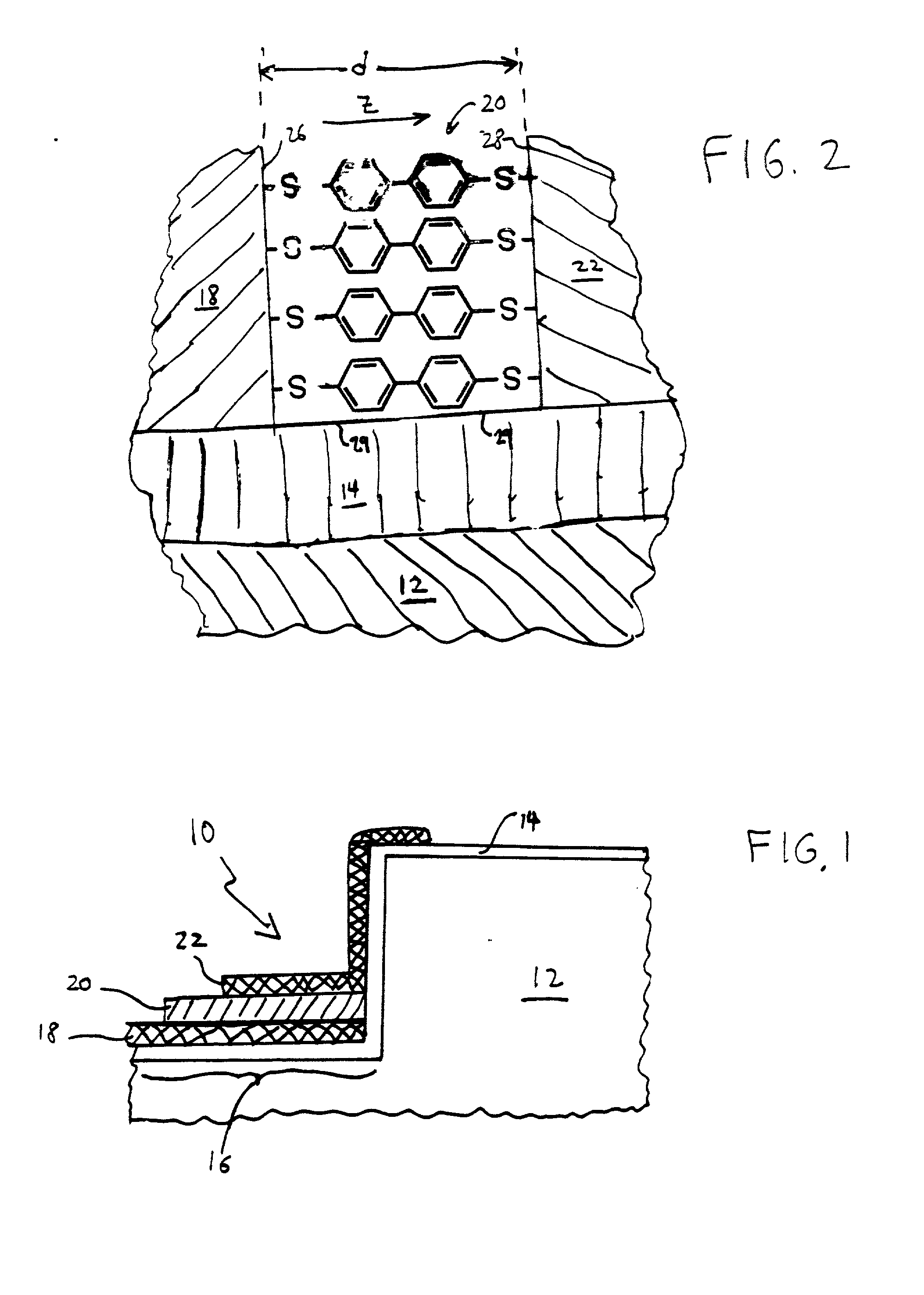
[0029] FIG. 1 shows an organic field-effect-transistor (OFET) 10 that forms a step-like structure on a conductive substrate 12. The step-like structure includes a dielectric layer 14 that covers a step on the substrate 12. The substrate 12 and dielectric layer 14 form a gate structure for the OFET 10. Exemplary substrates 12 include organic and inorganic conductors, e.g., a metal or heavily doped silicon that acts like a conductor. Exemplary dielectric layers 14 include inorganic and organic layers, e.g., layers of SiO.sub.2 or SiO.sub.2 (CH.sub.2).sub.NCO.sub.2.

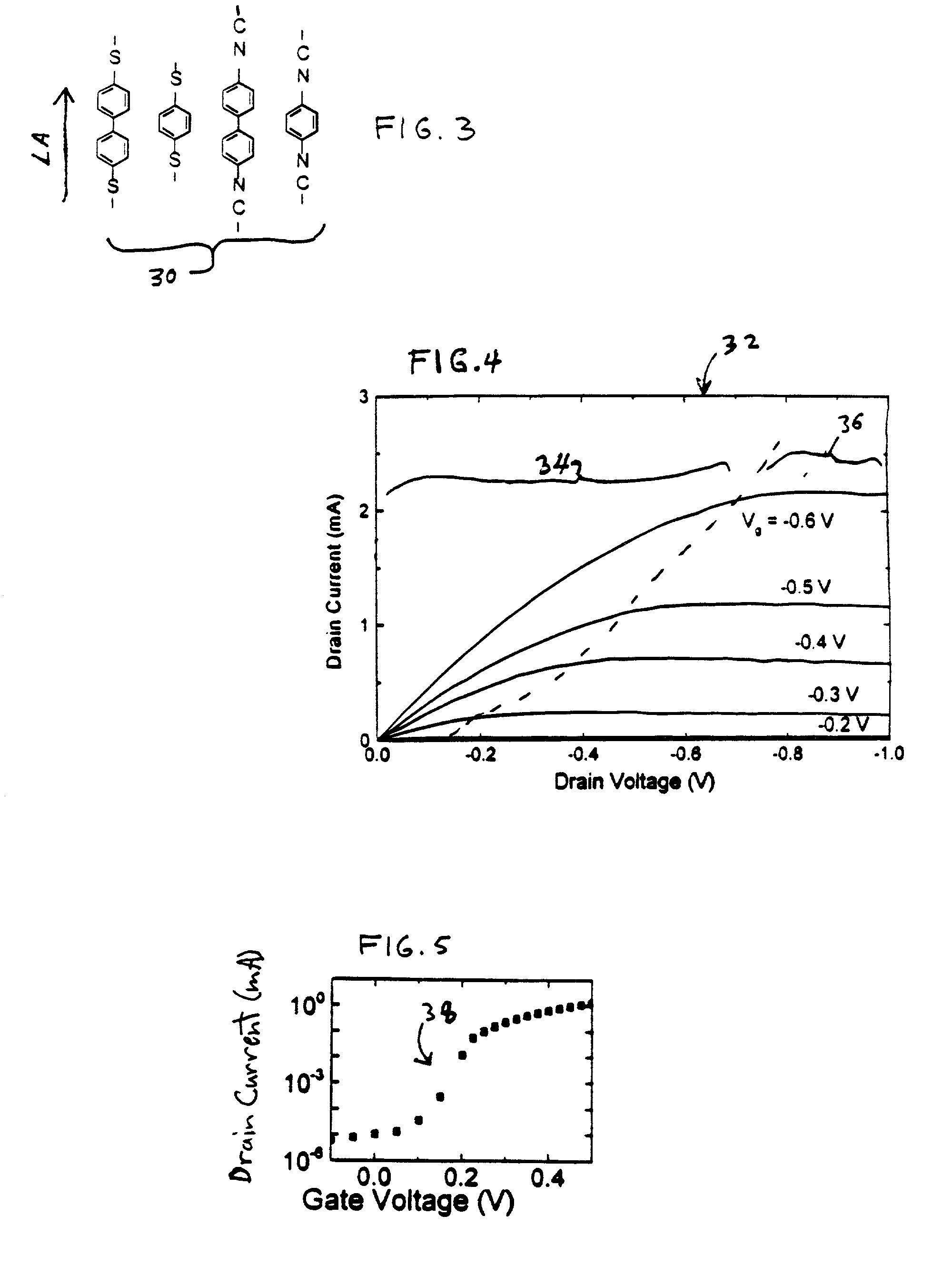
[0030] The step-like structure includes a horizontal region 16 covered by a stack-like channel structure. From the horizontal region 16 out, the stack-order of the channel-structure is dielectric layer 14, gold source electrode 18, active channel layer 20, and gold drain electrode 22. The active channel layer 20 includes one or more layers of aligned organic molecules that are aligned. The conductivity of the active channel ...


PUM

PropertyMeasurementUnit
lengthaaaaaaaaaa
lengthaaaaaaaaaa
lengthsaaaaaaaaaa

Abstract

A three-terminal device includes first electrode, second electrode, gate electrode and an active channel coupling the first and second electrodes. The active channel has a layer of organic molecules with conjugated multiple bonds. The delocalized pi-orbitals associated with the conjugated multiple bonds extend normal to the layer.

Description

[0001] 1. Field of the Invention[0002] The invention relates to semiconductor devices with active organic channels and three or more terminals.[0003] 2. Discussion of the Related Art[0004] Much interest in organic circuits stems from the availability of organic circuits with desirable mechanical properties and the availability of inexpensive fabrication techniques for such organic circuits. Exemplary of the desirable mechanical properties are mechanical flexibility, lightweightness, and ruggedness typically associated with circuits made with plastic substrates. Exemplary of the inexpensive fabrication techniques are reel-to-reel manufacture, solution-based deposition, feature printing, and lamination construction.[0005] Active organic devices have an organic semiconductor channel and three or more electrodes. The active organic semiconductor channel couples two of the electrodes and has a conductivity that is responsive to a voltage applied to a third one of the electrodes. The thir...

Claims


Application Information

Patent Timeline
Patent Type & Authority Applications(United States)
IPC IPC(8): H01L21/336H01L21/8236H01L27/088H01L27/28H01L29/78H01L29/786H01L51/00H01L51/05H01L51/30H01L51/40
CPCH01L27/28H01L51/0036H01L51/005H01L51/0053H01L51/057H01L51/007H01L51/0086H01L51/0545H01L51/0067H10K19/00H10K85/113H10K85/60H10K85/621H10K85/6565H10K85/344H10K85/654H10K10/491H10K10/466H01L29/78
Inventor BAO, ZHENANROGERS, JOHN A.SCHON, JAN HENDRIK
Owner LUCENT TECH INC
Why Eureka
Try Eureka