Circuit pattern of resistance heating elements and substrate-treating apparatus incorporating the pattern

a technology of resistance heating elements and substrates, which is applied in the field of ceramic heaters, can solve the problems of temperature distribution on the entire surface of upsized semiconductor wafers not being equalized within the required limit, and the temperature at the peripheral portion of the insulating substrates tending to decreas

Inactive Publication Date: 2002-12-12
SUMITOMO ELECTRIC IND LTD
View PDF0 Cites 19 Cited by
  • Summary
  • Abstract
  • Description
  • Claims
  • Application Information

AI Technical Summary

Problems solved by technology

However, with the above-described prior arts, the temperature distribution on the entire surface of the upsized semiconductor wafer cannot be equalized within the required limit.
Generally, the drawback of resistance-heating-element circuits embedded in an insulating substrate made of, for example, a ceramic material is that the temperature at the peripheral portion of the insulating substrate tends to decrease.

Method used


Image

  • Circuit pattern of resistance heating elements and substrate-treating apparatus incorporating the pattern
  • Circuit pattern of resistance heating elements and substrate-treating apparatus incorporating the pattern
  • Circuit pattern of resistance heating elements and substrate-treating apparatus incorporating the pattern

Examples


Embodiment Construction

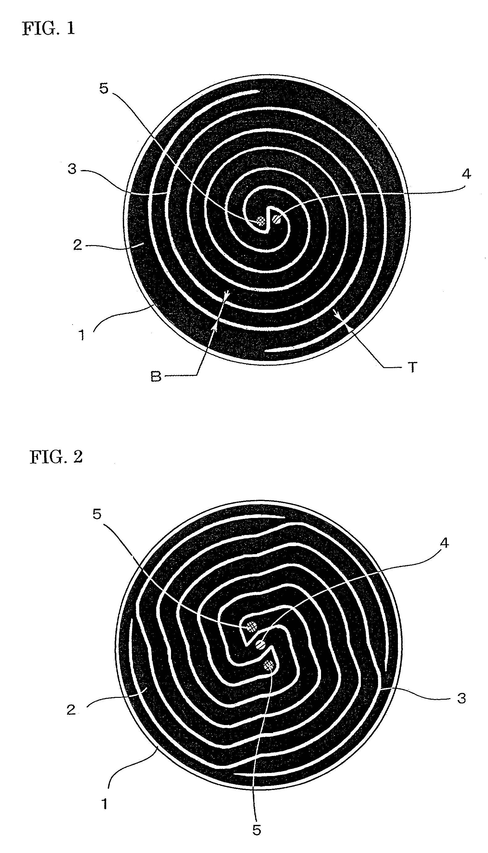
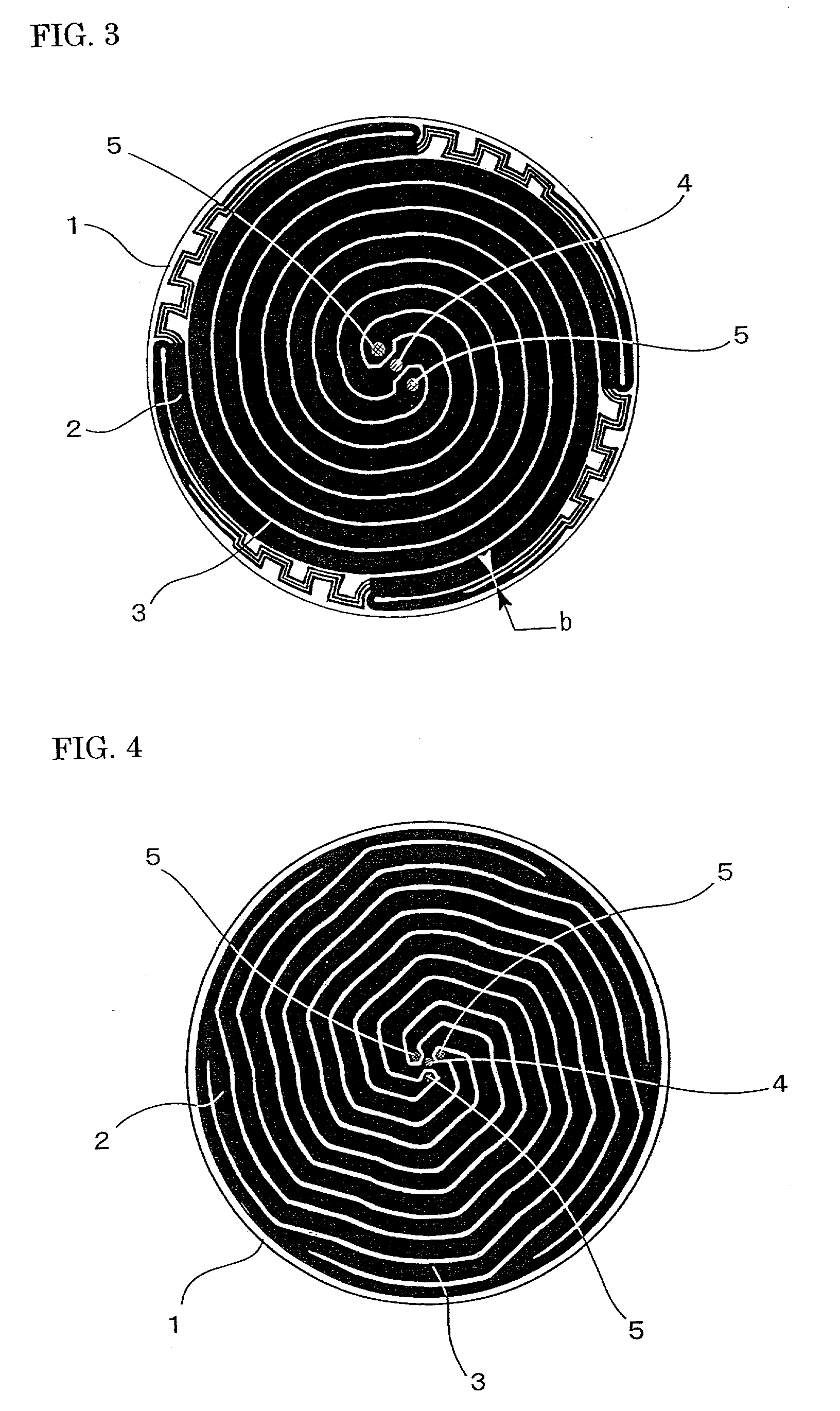
[0045] Samples shown in Table 2 were prepared to compare the present invention with the prior art shown in FIG. 8. The subject of the comparison is the uniformity of the temperature distribution produced by the individual circuit patterns of resistance heating elements. Four types of material powders, i.e., aluminum nitride, silicon nitride, alumina, and silicon carbide, were prepared as the ceramic materials for the insulating substrates. The ceramic material, a binder, a solvent, and a sintering agent as needed were mixed with a ball mill to produce a slurry. The slurry was formed into a green sheet by the doctor blade method. A resistance-heating-element circuit was formed on the green sheet by the screen-printing method using a tungsten paste.

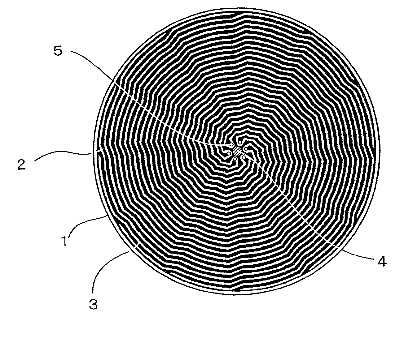
[0046] The circuit patterns of resistance heating elements employed were those shown in FIGS. 1 to 5 and 8. Table 1 shows the width B of the resistance-heating-element circuits and the space T between the adjacent resistance-heating-element...


PUM


Abstract

A technology that achieves a highly uniform temperature distribution on the surface of large-area semiconductor wafers and substrates for liquid crystals without prior measurement of the resistance-heating-element circuit and subsequent adjustment of the value of resistance. At least one current-receiving point 4 and at least one current-releasing point 5 are provided at the central portion of an insulating substrate 1. One or more resistance-heating-element circuits 2 are embedded in the insulating substrate spirally or pseudospirally from the central portion including the current-receiving point 4 to the peripheral portion of the insulating substrate 1. All the circuits merge with one another at the outermost portion. One or more resistance-heating-element circuits are separated at the outermost portion of the resistance-heating-element circuits and are formed spirally or pseudospirally from the outermost portion to the central portion including the current-releasing point 5.

Description

[0001] 1. Field of the Invention[0002] The present invention relates to a ceramic heater suitable for ensuring a uniform temperature distribution for treating semiconductor wafers, substrates for liquid crystals, etc. More specifically, it relates to a circuit pattern of resistance heating elements embedded in an insulating substrate and to a substrate-treating apparatus incorporating an insulating substrate in which resistance heating elements having the circuit pattern are embedded.[0003] 2. Description of the Background Art[0004] Layer formation and etching treatment are performed on a semiconductor wafer or a substrate for liquid crystals by using the chemical vapor deposition (CVD), physical vapor deposition (PVD), or sputtering method Ceramic heaters have been used to support these objects to be treated such as wafers and substrates and to heat them to a specified treating temperature. In recent years, these ceramic heaters have been increasingly used in a treating apparatus e...

Claims


Application Information

Patent Timeline
Patent Type & Authority Applications(United States)
IPC IPC(8): H01L21/00H05B3/20H01L21/02H01L21/324H05B3/10H05B3/14H05B3/28H05B3/68
CPCH01L21/67103H05B3/283H05B3/143H01L21/324
Inventor NATSUHARA, MASUHIRONARITA, MASASHINAKATA, HIROHIKOKUIBIRA, AKIRA
Owner SUMITOMO ELECTRIC IND LTD
Why Eureka
Try Eureka