Semiconductor wafer with ID mark, equipment for and method of manufacturing semiconductor device from them

a technology of semiconductor devices and id marks, which is applied in the testing/measurement of individual semiconductor devices, semiconductor/solid-state devices, instruments, etc., can solve the problems of relative large space loss of the wafer, markings that may disappear or become unrecognizable, and other problems, to achieve the effect of reducing the cost of the device, and improving the quality of the devi

Inactive Publication Date: 2003-01-02
KK TOSHIBA
View PDF15 Cites 299 Cited by
  • Summary
  • Abstract
  • Description
  • Claims
  • Application Information

AI Technical Summary

Benefits of technology

[0392] Additional advantages and modifications of the present invention will readily occur to those skilled in the art. Therefore, the present invention in its broader aspects is not limited to the specific details and representative first to ninth embodiments shown and described herein. Accordingly, various modifications may be made without departing from the spirit or scope of the general inventive concept as defined by the appended claims and their equivalents.

Problems solved by technology

The marking must be visible to workers, and therefore, usually extends from several millimeters to several centimeters causing relatively large space loss on the wafer.
When the marking are formed on the surface of a wafer, the marking may disappear or become unrecognizable due to repetitive deposition and chemical mechanical polishing (CMP) processes carried out on the wafer.
When the marking are formed on the back of a wafer, irregularities in the marking may cause focal errors in a lithography process and will impose the additional work of reversing the wafer in order to see the marking.
The related arts, however, also have problems.
As a result, the processing conditions set for a batch of wafers involve redundancies such as a too long process time, deteriorating productivity and increasing costs.
It is difficult for the related arts to utilize, for example, film thicknesses measured on individual wafers to determine processing conditions applied to the wafers in the next manufacturing process.

Method used


Image

  • Semiconductor wafer with ID mark, equipment for and method of manufacturing semiconductor device from them
  • Semiconductor wafer with ID mark, equipment for and method of manufacturing semiconductor device from them
  • Semiconductor wafer with ID mark, equipment for and method of manufacturing semiconductor device from them

Examples


first embodiment

[0107] First Embodiment

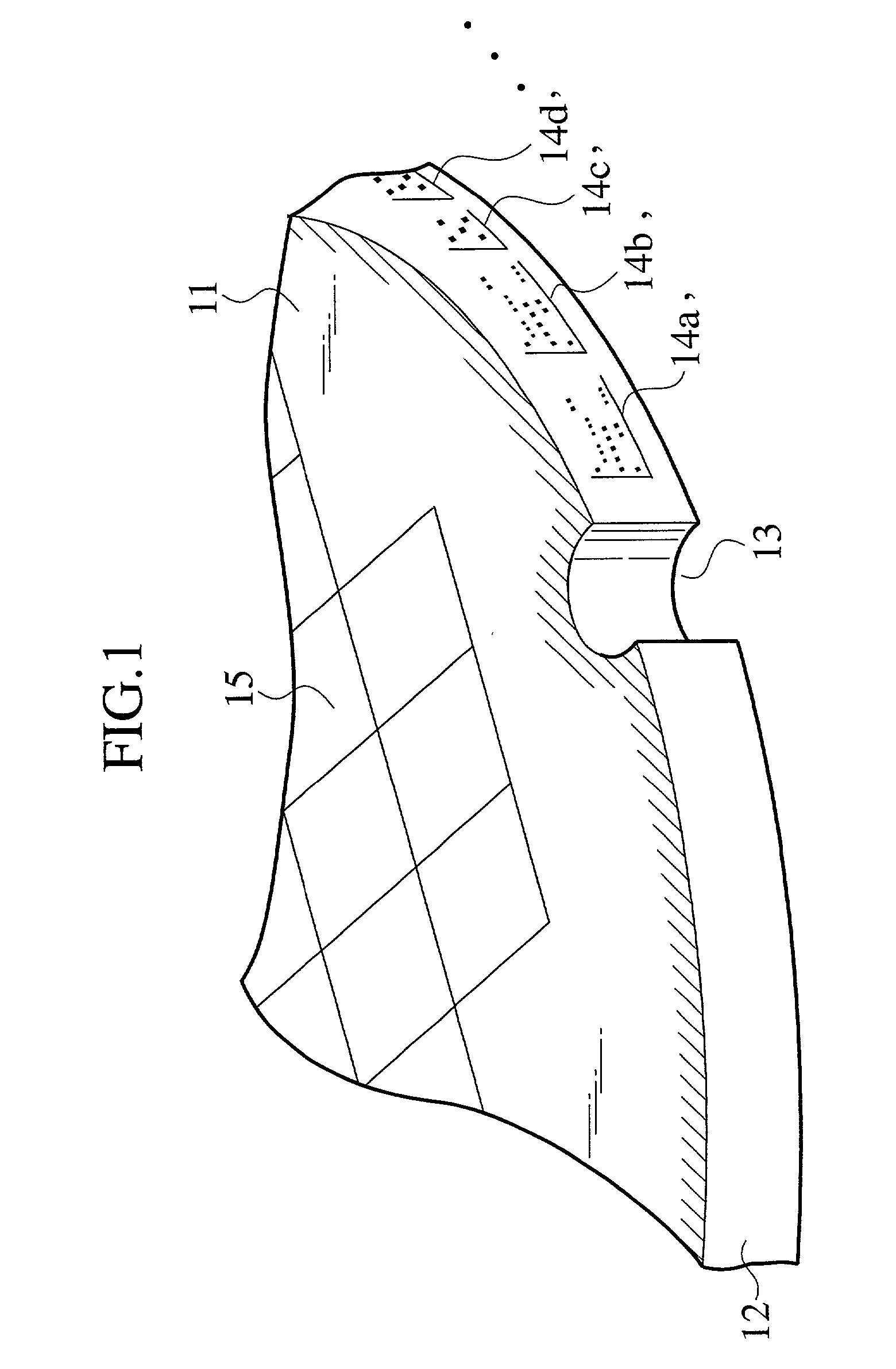
[0108] In FIG. 1, the wafer 11 has a bevel contour 12 along the periphery of the wafer 11, products 15 formed on the wafer 11, and ID marks 14a to 14d formed on the bevel contour 12. The ID marks 14a to 14d indicate product data such as the properties, manufacturing conditions, and test results of the products 15. Whenever required, any manufacturing process may form an ID mark on the bevel contour 12 of the wafer 11, and therefore, the number of ID marks on the bevel contour 12 is optional. The ID marks may contain, for example, the lot number, manufacturing number, functions, and test results of the products 15.

[0109] The "periphery" of the wafer 11 includes an area where the bevel contour 12 is formed, a surface circumferential area of the wafer 11 where no products 15 are formed, the side face of the wafer 11, and a back circumferential area of the wafer 11. The products 15 are any products formed on the wafer 11 through a series of semiconductor device ma...

second embodiment

[0153] Second Embodiment

[0154] The first embodiment and modifications do not particularly specify a location in a bevel contour of a wafer where an ID mark is formed. An ID mark must sometimes be made at the outermost part of a bevel contour of a wafer. If an ID mark is close to products formed on a wafer, the ID mark may be erased during a CMP process that is frequently carried out in semiconductor device manufacturing. To avoid erasure by CMP processing, ID marks must be formed at the outermost part of a bevel contour of a wafer. The second embodiment of the present invention relates to the locations and number of ID marks to be formed on a bevel contour of a wafer.

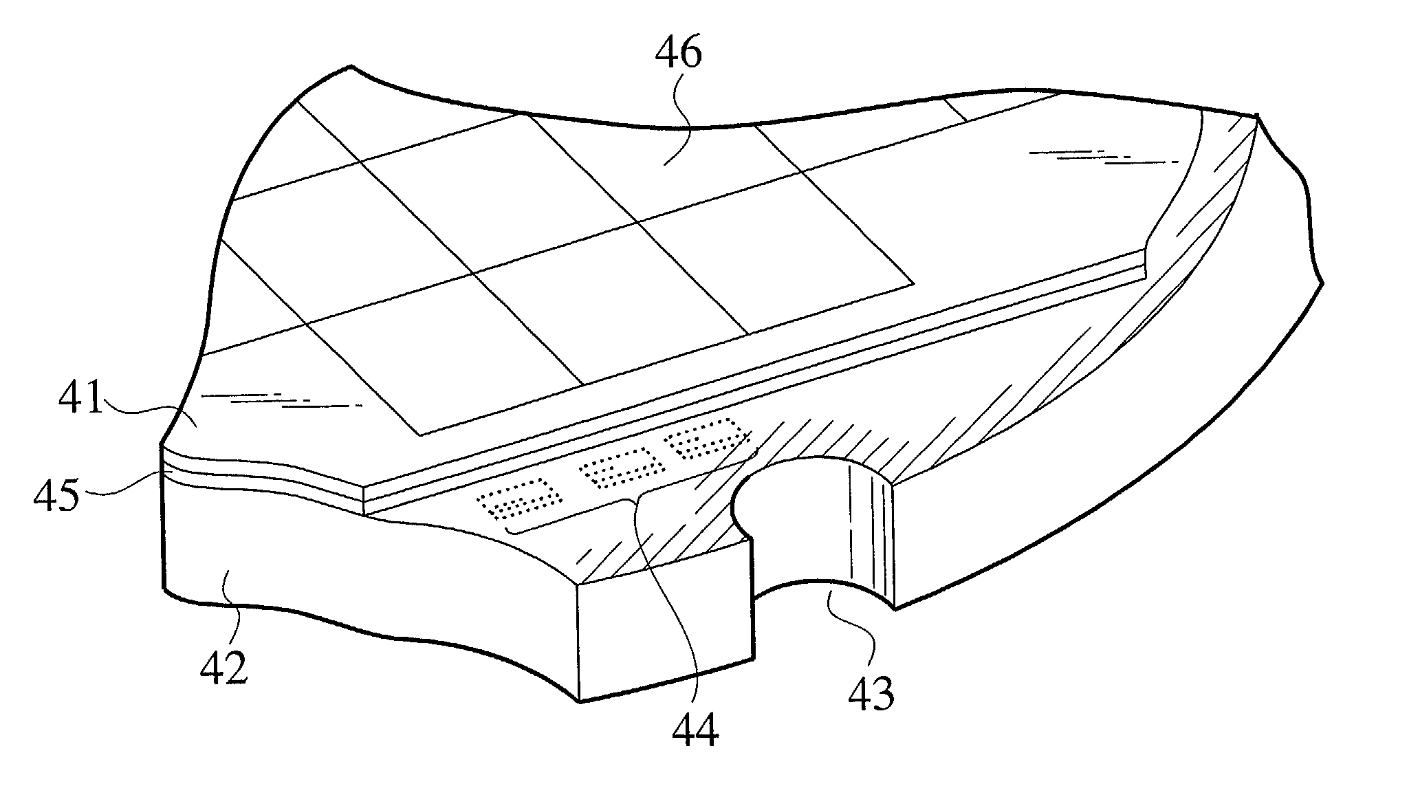
[0155] In FIG. 5, the wafer 21 has a notch 23 formed on a bevel contour 22 extending along the periphery of the wafer 21. With respect to the notch 23 serving as a reference, three ID marks 24a to 24c having the same contents are formed on the bevel contour 22. Each ID mark has a rectangular shape of 30 .mu.m.times.140 ...

third embodiment

[0171] Third Embodiment

[0172] In FIG. 10, the wafer 34 has a reference position 36 and ID marks 37 and 38 formed on each side of the reference position 36. The reference position 36 is an object or a mark indicating a crystal orientation of the wafer 34. The reference position 36 is, for example, an orientation flat, a notch, or a mark. In FIG. 10, the ID mark 37 is a manufacture number formed by a wafer maker and the ID mark 38 is a mark formed by a device maker. The ID marks 37 and 38 are formed on the left and right sides of the reference position (notch) 36, respectively.

[0173] In FIG. 11, a wafer 34 according to a comparison example has a notch 36 serving as a reference position and ID marks 39 and 40 formed on the same side of the notch 36. The ID marks 39 and 40 are formed by a wafer maker and a device maker, respectively.

[0174] Compared with the comparison example of FIG. 11, the third embodiment of FIG. 10 can shorten an ID mark read time. The reason for this will be explai...


PUM


Abstract

A semiconductor wafer has a bevel contour formed along the periphery thereof, products formed on the wafer, and an ID mark formed on the bevel contour. The ID mark shows at least the properties, manufacturing conditions, and test results of the products.

Description

[0001] This application is based upon and claims the benefit of priority from the prior Japanese Patent Applications No. P2001-80452 filed on Mar. 21, 2001 and No. P2001-345984 filed on Nov. 12, 2001, the entire contents of which are incorporated herein by reference.[0002] 1. Field of the Invention[0003] The present invention relates to a semiconductor wafer having an ID mark on the periphery thereof and a method of manufacturing such a semiconductor wafer. The present invention also relates to an equipment for and a method of manufacturing semiconductor device from such a semiconductor wafer.[0004] 2. Description of the Related Art[0005] Semiconductor device manufacturing involves several hundreds of processes each of which needs different conditions that must be strictly managed. Management of the process conditions of wafers employs markings made on the wafers. These markings consist of, for example, numerals, characters, and bar codes.[0006] A marking on a semiconductor wafer is...

Claims


Application Information

Patent Timeline
Patent Type & Authority Applications(United States)
IPC IPC(8): H01L23/544H01L21/02
CPCH01L23/544H01L2223/54406H01L2223/54413H01L2223/54433H01L2223/54493H01L2924/0002Y10S438/974H01L2924/00H01L21/02
Inventor ARIKADO, TSUNETOSHIIWASE, MASAONADAHARA, SOICHIUDO, YUSOUSHIKU, YUKIHIRONITTA, SHINICHIMIYASHITA, MORIYASUGAMOTO, JUNJIYAMADA, HIROAKINAGANO, HAJIMETANZAWA, KATSUJIROMATSUSHITA, HIROSHITSUCHIYA, NORIHIKOOKUMURA, KATSUYA
Owner KK TOSHIBA
Why Eureka
Try Eureka