[0032] While the description above provides a full and complete disclosure of the preferred embodiments of the present invention, various modifications, alternate constructions, and equivalents will be obvious to those with skill in the art. Thus the scope of the present invention is limited solely by the appended claims.
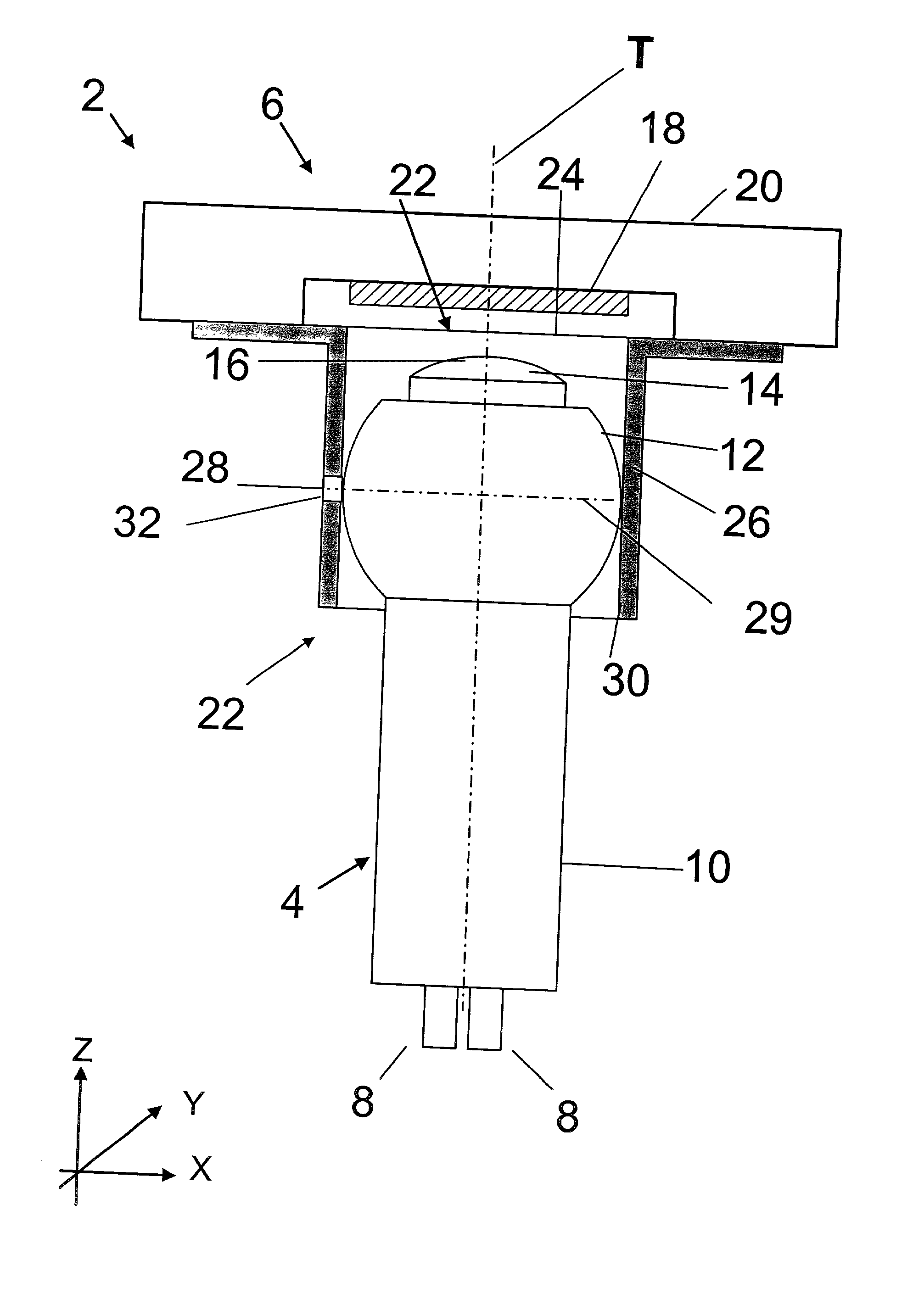
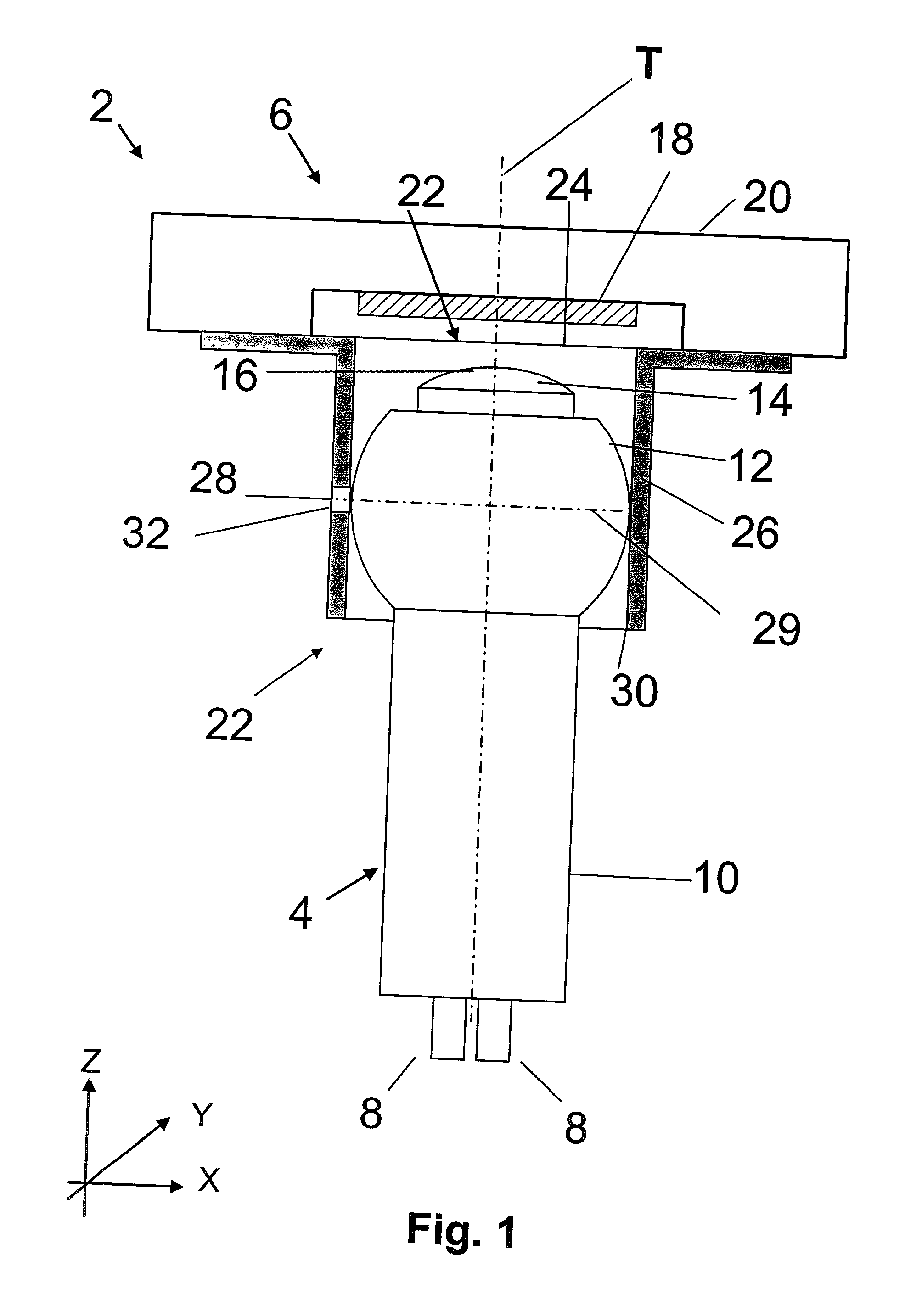
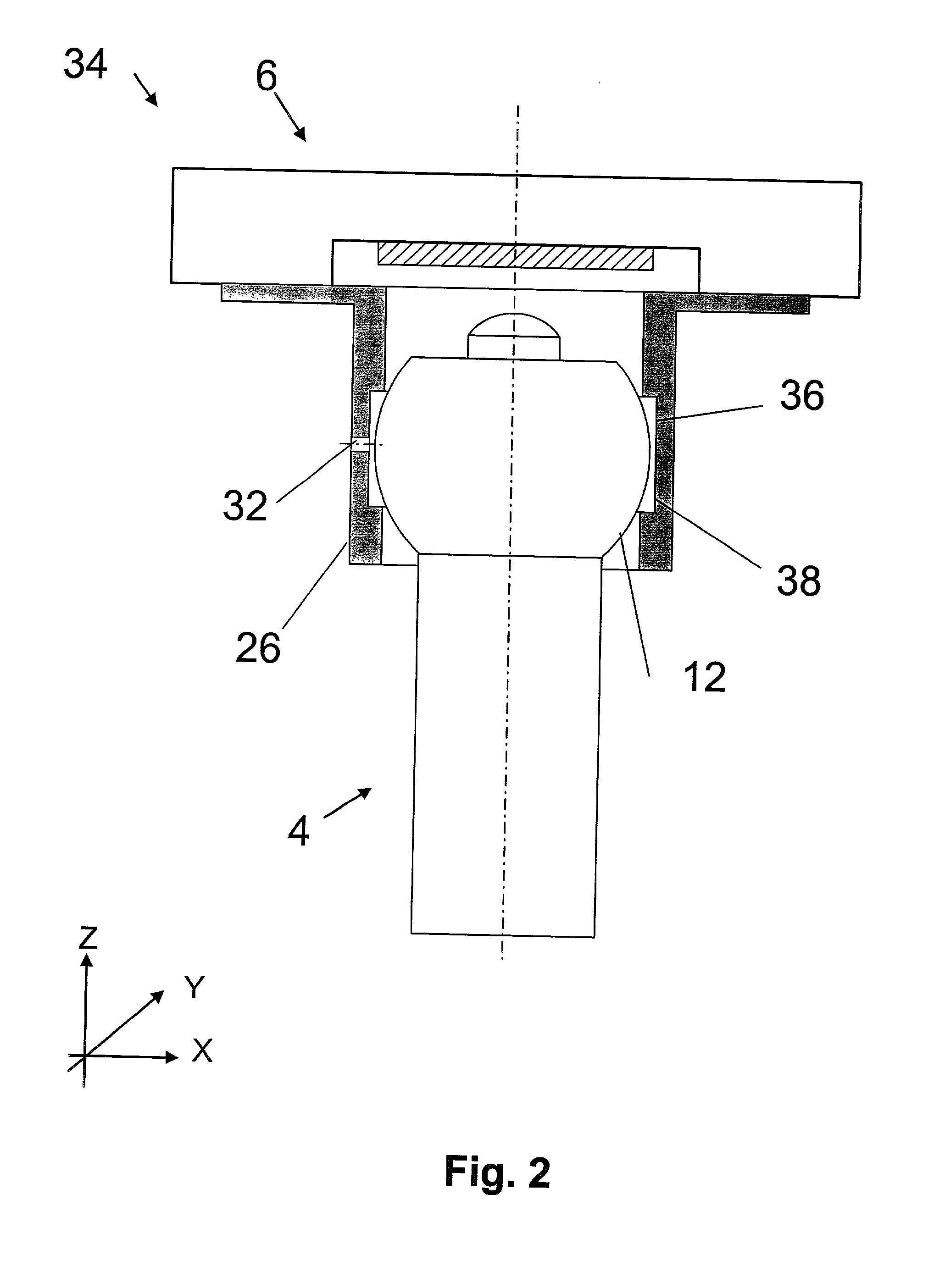
[0033] Referring now generally to the Figures and particularly to FIG. 1, a first preferred embodiment of the present invention, or photonic package 2. The photonic package 2 includes a first photonic component 4 and a second photonic component 6. The first photonic component 4 has an optical fiber 8 and a first housing 10 having a partially spherical surface 12. The partially spherical surface 12 is partially spherical and includes a first photonic opening 14. The first photonic opening 14 permits light to pass in and out of an endface 16 of the optical fiber 8. The second photonic component 6 has a MEMS optical mirror die 18, a second housing 20 and an access port 22. The second housing 20 is coupled to the MEMS optical mirror die 18, or MEMS die 18, and substantially encloses and protects the MEMS die 18. The access port 22 includes an access opening 24 and a cylindrical contact surface 26. The access opening 24 permits light to pass to and from the MEMS die 18. A contact area 28 of the cylindrical contact surface 26 is shaped and sized to mechanically contact at least part of the partially spherical surface 12. The cylindrical contact surface 26 allows, while the partially spherical surface 12 is in contact with the contact area 28, linear motion of the spherical surface 12 along a Z axis and constrains the movement of the partially spherical surface 12 in a mutually orthogonal X linear axis and Y linear axis. The partially spherical surface 12 may, however, be moved along the Z axis and be rotated about the X, Y and Z axis while the partially spherical surface 12 is inserted within the cylindrical contact surface 26. The first photonic component 4 may be aligned by inserting the partially spherical surface within the cylindrical contact surface 26 and then linearly moved in the Z axis and rotated until an acceptable, desired or optimal alignment of the first photonic component 4 and the second photonic component 6 is achieved.
[0034] The partially spherical surface 12 of the first photonic component 4 is inserted into the access port 22 and positioned against the cylindrical contact surface 26. The partially spherical surface 12 forms a seal line 29 with the cylindrical contact surface 26. The seal line 29 is maintained as the partially spherical surface 12 is rotated and moved along the Z axis. The first photonic component 4 is thereby positioned into an acceptable or optimal alignment with the second photonic component 6. Once the first photonic component 4 and the second photonic component 6 are acceptably aligned, the first photonic component 4 and the second photonic component 6 are permanently assembled together by affixing or adhering the first photonic component 4 and the second photonic component 6 at and/or proximate to the seal line 29. The quality of an alignment may be evaluated by transmitting an optical signal between the optical fiber 8 and the MEMS die 18 and comparing a resulting received signal of this transmission with an expected received signal achievable when the first photonic component 4 and the second photonic component 6 are in a desirable or an optimal alignment. When the first photonic component 4 and the second photonic component 6 have achieved an acceptable, desirable or optimal alignment, the cylindrical contact surface 26 and the partially spherical surface 12 may be affixed together in a desired alignment by a suitable process or form of coupling known in the art, to include heating and cooling, adhering, adhering with epoxy, soldering, welding, solid phase welding, thermal compression welding, acoustic welding, spot welding, spark welding, laser welding, electrical welding and mechanical contact welding. An optional layer of material 30, such as an adhesive, solder, an epoxy, or a welding material used in welding such as Gold or one of a group of suitable weld filler materials or metals known in the art, may be deposited on either the partially spherical surface 12 or the cylindrical contact surface 26 prior to the insertion of the partially spherical surface 12 into the access port 22. The layer of material 30 is then used to affix, adhere, weld or solder the first photonic package 4 to or with the second photonic package 6.
[0035] An axis T is an optical axis of the first photonic component and/or the second photonic component or parts thereof, for example the MEMS die 18 or the optical fiber 8. The first photonic component 4 and the second photonic component 6 are substantially symmetric about the T optical axis.
[0036] Alternate variations of the photonic package 2 include additional or alternate photonic elements coupled with the first housing 10 of the first photonic component 4 or the second housing 20 of the second photonic component 6, to include an additional individual or a plurality of optical fibers or wave guides. One or more mirrors, prisms, wave guides, optical fibers, lenses, collimators, and other suitable photonic and optical devices and elements known in the art are additionally or alternately coupled to either or both the first housing and the second housing 20 in certain preferred variations of the photonic package. A coupled lens may be a suitable optical lens, spherical lens, aspherical lens, ball lens, GRIN lens, C-lens or lens system known in the art. Suitable optical fibers, planar wave guides, photonic crystal wave guides, and/or other suitable channels for optical signal and light energy transmission known in the art may be coupled with either or both the first housing 10 and the second housing 20. Additionally or alternatively, an optical or photonic element, or a plurality of optical or photonic elements, may be coupled to either photonic components 4 & 6, where each photonic element selected from the group consisting of a wave guide, a planar wave guide, a photonic crystal wave guide, a diffraction wave guide grating, an optical fiber, a collimator, a lens, a diffractive lens, an optical lens, a spherical lens, an aspherical lens, a ball lens, a lens, a C-lens, a lens system, a mirror, a flat mirror, a shaped mirror, a diffractive mirror, a grating plate or plates, a laser, a modulator, a photodiode, a VCSEL, a prism, and other suitable photonic or optical devices or elements known in the art.
[0037] A hole 32 of the cylindrical contact surface 26 allows for the material 30, such as a welding material, an adhesive, epoxy or solder, to be introduced to the contact area 28 of the cylindrical contact surface 26 before or after the partially spherical surface 12 is substantially in mechanical contact with the cylindrical contact surface 26. The material 30 may be introduced as the partially spherical surface 12 is being moved or aligned, and/or after the partially spherical surface 12 has been aligned as desired for assembly with the second photonic component 6. The assembly of the first photonic component 4 with the second photonic component 6 is advanced by the delivery of the material 30 through the hole 32 at a time chosen to support a desirable alignment of the first photonic component 4 and the second photonic component 6 at the seal line 29 where the spherical surface 12 mechanically touches the cylindrical contact surface 26.
[0038] In alternate preferred embodiments the first component 4 may have an ovoid, ellipsoid or other suitable convex surface that couples with the contact surface 26 of the second housing 20 in addition to as an alternative to the partially spherical surface.
[0039] Referring now generally to the Figures and particularly to FIG. 2, FIG. 2 is a cross-sectional view of a second preferred embodiment of the present invention 34, or rigid photonic package 34, having the cylindrical contact surface 26 with an internal niche 36. The niche 36 may be sized and fitted with relatively planar sides 38 or convex sides, and the niche 36 may be lengthened or shortened to permit the partially spherical surface 12 a range of linear Z motion while held with the niche 36. The cylindrical contact surface 26 is made of a semi-flexible material that allows the partially spherical surface 12 to deform and expand to allow the partially spherical surface 12 to be inserted into the access port 22 and partially within the cylindrical contact surface 26 to be placed into the internal niche 36. Alternatively, the partially spherical surface 12, or both the partially spherical surface 12 and the cylindrical contact surface 26, may be made of a semi-flexible material that allows the partially spherical surface to be deformed and compressed to allow the partially spherical surface 12 to squeeze partially through the cylindrical contact surface 26 and into the niche 36. Once the partially spherical surface 12 is located within the niche 36 the first photonic component 4 is next positioned into a desirable orientation in relation to the second photonic component 6. The first photonic component 4 and the second photonic component 6 are then formed or affixed into a rigid photonic package 34 by welding or adhering, or another suitable assembly formation method known in the art.
[0040] Referring now generally to the Figures and particularly to FIG. 3, FIG. 3 is a cross-sectional view of a third preferred embodiment of the present invention 40 having a conical contact surface 42. The partially spherical surface 12 of the first photonic component 4 is inserted into the access port 22 and positioned against the conical contact surface 42. The partially spherical surface 12 forms the seal line 29 with the conical contact surface 42. The seal line 29 is maintained as the partially spherical surface 12 is rotated and the first photonic component 4 is positioned into a desirable alignment with the second photonic component 6. Once the first photonic component 4 and the second photonic component 6 are acceptably aligned, the first photonic component 4 and the second photonic component 6 are permanently assembled together by affixing or adhering the first photonic component 4 and the second photonic component 6 at and/or proximate to the seal line 29. The first photonic component 4 and the second photonic component 6 may be affixed or adhered together by suitable methods and means known in the art, such as adhering, adhering with epoxy, soldering, welding, solid phase welding, thermal compression welding, acoustic welding, spot welding, spark welding, laser welding, electrical welding and mechanical contact welding.
[0041] Referring now generally to the Figures and particularly to FIG. 4, FIG. 4 is a cross-sectional view of a fourth preferred embodiment of the present invention 44, or para-spherical photonic package 44, having a para-spherical contact surface 46. The partially spherical surface 12 is mechanically in contact with a contact area 48 of the para-spherical contact surface 46 during alignment and assembly of the para-spherical photonic package 44. The para-spherical contact surface 46 constrains, while the partially spherical surface 12 is partially or substantially fitted within the para-spherical contact surface 46, the movement of the partially spherical surface 12 in the X and Y linear axis in both directions and along the linear Z axis along the direction towards the second photonic component 6. The partially spherical surface 12 may, however, rotate about the X, Y and Z axis while the partially spherical surface 12 is in mechanical contact with the para-spherical contact surface 46. The first photonic component 4 may be aligned by placing or pressing the partially spherical surface 12 onto the para-spherical contact surface 46 and then rotating the first photonic component 4 until the desired alignment with the second photonic component 6 is achieved.
[0042] Referring now generally to the Figures and particularly to FIG. 5, FIG. 5 is a cross-section of a fifth preferred embodiment of the present invention 48, or spherical photonic package 48. The spherical photonic package 48 includes the first photonic component 4 having a first internal photonic element 50, the first housing 10 and the partially spherical surface 12. The partially spherical surface 12 includes the first photonic opening 14. The first photonic opening 14 permits light to pass to and from the first photonic element 50. The second photonic component 6 has a second internal photonic element 52, the second housing 20 and the access port 22. The second housing 20 is coupled to the second internal photonic element 52 and substantially encloses and protects the second internal photonic element 52. The access port 22 includes an access opening 24 and a contact surface 54. The access opening 24 permits light to pass to and from the second internal photonic element 52. The contact surface 54 is shaped and sized to mechanically contact and substantially or partly enclose at least part of the partially spherical surface 12. The contact surface 54 and the partially spherical surface 12 are sized and shaped to enable the partially spherical surface 12 to snap fit within the contact surface 54. The partially spherical surface 12 is mechanically in contact with a contact area 56 of the contact surface 54 during alignment and assembly of the spherical photonic package 48. The contact surface 54 constrains the movement of the partially spherical surface 12 in the X and Y linear axis and the linear Z axis while the partially spherical surface 12 is partially or substantially fitted within the contact surface 54. The partially spherical surface 12 may, however, rotate about the X, Y and Z axis while the partially spherical surface 12 is in mechanical contact with the concave spherical contact area 56. The first photonic component 4 may be aligned by placing or pressing the partially spherical surface 12 into the contact surface 54 and then rotating the first photonic component 4 until the desired alignment with the second photonic component 6 is achieved, and whereby a desired, preferred or optimized alignment of the first internal photonic element 50 and the second internal photonic element 52 is achieved. In certain alternate preferred embodiments, the partially spherical surface 12 may be partially ellipsoid or ovoid, and/or have at least one at least partially circular, elliptical or oval cross-section.
[0043] The contact surface 54 and/or the partially spherical surface 12 are made of semi-flexible material that deforms, expands or compresses sufficiently to enable the partially spherical surface 12 to be inserted partially into the access port 22 and to be constrained by the contact surface 54. The partially spherical surface 12 and the contact surface 54 may then be affixed together in a desired alignment by a suitable form of stationary coupling known in the art, to include heating and cooling, adhering, adhering with epoxy, soldering, welding, solid phase welding, thermal compression welding, acoustic welding, spot welding, spark welding, laser welding, electrical welding and mechanical contact welding. The contact surface 54 has an optional thinned edge 58 that promotes the welding of the contact surface 54 to the partially spherical surface 12 by electrical current welding techniques.
[0044] Referring now generally to the Figures and particularly to FIG. 6, FIG. 6 is a cross-sectional view of a sixth preferred embodiment 60 of the present invention having a second photonic component 6 with a partially spherical domed wall 62. A convex partially spherical surface 64 of the first photonic component 4 is shaped and sized to make mechanical contact with the spherical domed wall 62 and to allow the first photonic component 4 to be rotated by slidably positioning the convex partially spherical surface 64 about the spherical domed wall 62. The convex partially spherical surface 64 has a thinned edge 66 that improves the effectiveness of electrically welding the convex partially spherical surface 64 to the spherical domed wall 62. Alternatively, once the first photonic component 4 and the second photonic component 6 are desirably aligned, the convex partially spherical surface 64 and the partially spherical domed wall 62 may be affixed or adhered together by soldering, applying adherents, or another suitable affixing or welding technique known in the art.
[0045] Referring now generally to the Figures and particularly to FIG. 7, FIG. 7 is a cross-section of a seventh preferred embodiment of the present invention 68, or dual spherical photonic package 68. The dual spherical photonic package 68 is or comprises an assembly of the first photonic component 4 of FIG. 1, a modified second photonic component 70 and a third photonic component 72. The modified second photonic 70 and the third photonic component 72 are asymmetric about an optical axis W of the first photonic component 4. The third photonic component 72 has a third internal photonic element 73, a third housing 74 and an ancillary partially spherical surface 75, or ancillary surface 75. The modified second photonic component 70 has the contact surface 54 and a second contact surface 76. The second contact surface 76 is shaped and sized to mechanically contact and substantially or partly enclose at least part of the ancillary surface 75. The second contact surface 76 and the ancillary surface 75 are sized and shaped to enable the ancillary surface 75 to snap fit within the second contact surface 76. The ancillary surface 75 is mechanically in contact with a contact area 78 of the second contact surface 76 during alignment and assembly of the dual spherical photonic package 68. The second contact surface 76 constrains the movement of the ancillary surface 75 in the X and Y linear axis and the linear Z axis while ancillary surface 75 is partially or substantially fitted within the second contact surface 76. The ancillary surface 75 may, however, rotate about the X, Y and Z axis while the ancillary surface 75 is in mechanical contact with the concave spherical contact area 78. The third photonic component 72 may be aligned by placing or pressing the ancillary surface 75 into the second contact surface 76 and then rotating the third photonic component 72 until the desired alignment between the modified second photonic component 70 is achieved, whereby a desired, preferred or optimized alignment of the second internal photonic element 52 and the third internal photonic element 73 is achieved. In certain alternate preferred embodiments, the ancillary surface 75 may be partially ellipsoid or ovoid, and/or have at least one at least partially circular, elliptical or oval cross-section.
[0046] The present invention has been described in conjunction with the preferred embodiments. Although the present invention has been described with reference to specific exemplary embodiments, it will be evident that various modifications and changes may be made to these embodiments without departing from the broader spirit and scope of the invention as set forth in the claims. Accordingly, the specification and drawings are to be regarded in an illustrative rather than a restrictive sense. As noted above, the present invention is applicable to the use, operation, structure and fabrication of a number of different photonic component assemblies. The present invention should not be considered limited to the particular examples described above, but rather should be understood to cover all aspects of the invention as fairly set out in the attached claims. Various modifications, equivalent processes, as well as numerous structures to which the present invention may be applicable will be readily apparent to those of skill in the art to which the present invention is directed upon review of the present specification. The claims are intended to cover such modifications, devices and methods.